


 |
市場調查報告書
商品編碼
1684518
光刻計量設備市場機會、成長動力、產業趨勢分析與預測 2025 - 2034Lithography Metrology Equipment Market Opportunity, Growth Drivers, Industry Trend Analysis, and Forecast 2025 - 2034 |
||||||
2024 年全球光刻計量設備市場規模達到 7.55 億美元,預計在 2025 年至 2034 年期間將以 7.4% 的驚人複合年成長率成長。這些設備依賴緊湊、高性能積體電路 (IC),對尖端的光刻製程至關重要。這些先進的技術對於實現更高的晶片密度至關重要,而更高的晶片密度對於滿足消費者和產業對下一代功能的要求是必不可少的。此外,人們對半導體製造、5G 技術採用和人工智慧應用創新的日益關注也推動了對精密計量解決方案的需求。製造商正在加大對最先進設備的投資,以滿足優先考慮生產過程準確性和效率的行業不斷變化的需求。
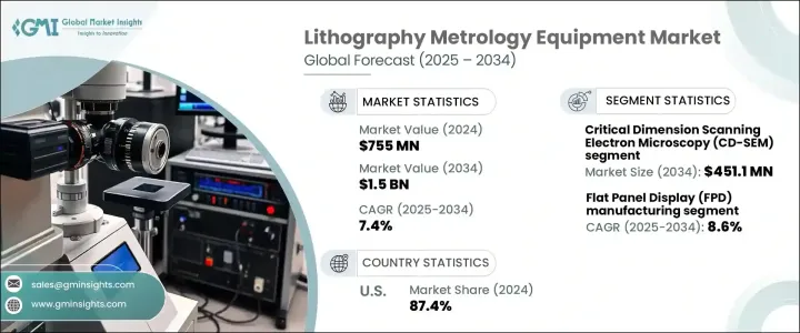
根據技術,市場分為覆蓋計量、原子力顯微鏡 (AFM)、臨界尺寸掃描電子顯微鏡 (CD-SEM)、光學計量和散射測量。其中,CD-SEM 將佔據主導地位,預計到 2034 年其市場價值將達到 4.511 億美元。該技術可確保在檢查掩模圖案、光刻結構和複雜設計時具有無與倫比的精度,從而實現高度小型化和複雜的半導體生產。對下一代晶片日益成長的需求推動了 CD-SEM 技術的進步,重點是實現更高的解析度、更高的吞吐量和增強的自動化以滿足行業標準。
| 市場範圍 | |
|---|---|
| 起始年份 | 2024 |
| 預測年份 | 2025-2034 |
| 起始值 | 7.55億美元 |
| 預測值 | 15億美元 |
| 複合年成長率 | 7.4% |
市場根據應用進一步分類,包括 LED 製造、半導體製造、平板顯示器 (FPD) 製造、MEMS(微機電系統)等。 FPD 製造業預計將經歷最高的成長,2025 年至 2034 年的複合年成長率為 8.6%。這些工具在測量層厚度、對準和解析度方面發揮關鍵作用,確保最佳的顯示性能和質量,這對於保持電子市場的競爭優勢至關重要。
在美國,光刻計量設備市場在 2024 年佔據了 87.4% 的佔有率。對包括 5nm 及更高技術節點在內的尖端節點的投資正在加速 EUV 光刻和先進計量解決方案的採用。此外,對 3D 封裝技術的日益關注以及人工智慧、物聯網和 5G 的廣泛應用,進一步推動了美國對創新和精密光刻計量設備的需求。
目錄
第 1 章:方法論與範圍
- 市場範圍和定義
- 基礎估算與計算
- 預測計算
- 資料來源
- 基本的
- 次要
- 付費來源
- 公共資源
第 2 章:執行摘要
第 3 章:產業洞察
- 產業生態系統分析
- 影響價值鏈的因素
- 利潤率分析
- 中斷
- 未來展望
- 製造商
- 經銷商
- 供應商概況
- 利潤率分析
- 重要新聞及舉措
- 監管格局
- 衝擊力
- 成長動力
- 半導體技術的進步
- 消費性電子產品需求不斷成長
- 5G 和人工智慧 (AI) 應用的成長
- 越來越關注代工和內存製造
- 光學和非光學計量技術進步
- 產業陷阱與挑戰
- 先進計量設備成本高昂
- 測量先進節點的複雜性
- 成長動力
- 成長潛力分析
- 波特的分析
- PESTEL 分析
第4章:競爭格局
- 介紹
- 公司市佔率分析
- 競爭定位矩陣
- 戰略展望矩陣
第 5 章:市場估計與預測:按技術,2021 年至 2034 年
- 主要趨勢
- 光學計量
- 臨界尺寸掃描電子顯微鏡 (CD-SEM)
- 疊層測量
- 原子力顯微鏡 (AFM)
- 散射測量
第 6 章:市場估計與預測:按產品,2021-2034 年
- 主要趨勢
- 化學控制設備
- 瓦斯控制設備
- 其他
第 7 章:市場估計與預測:按工藝,2021 年至 2034 年
- 主要趨勢
- 邊緣
- 雲
第 8 章:市場估計與預測:按應用,2021 年至 2034 年
- 主要趨勢
- 半導體製造
- 平面顯示器(FPD)製造
- MEMS(微機電系統)
- LED 製造
- 其他
第 9 章:市場估計與預測:按最終用途產業,2021 年至 2034 年
- 主要趨勢
- 整合設備製造商 (IDM)
- 鑄造廠
第 10 章:市場估計與預測:按地區,2021 年至 2034 年
- 主要趨勢
- 北美洲
- 美國
- 加拿大
- 歐洲
- 英國
- 德國
- 法國
- 義大利
- 西班牙
- 俄羅斯
- 亞太地區
- 中國
- 印度
- 日本
- 韓國
- 澳洲
- 拉丁美洲
- 巴西
- 墨西哥
- 中東及非洲
- 南非
- 沙烏地阿拉伯
- 阿拉伯聯合大公國
第 11 章:公司簡介
- ASML Holding NV
- Advantest Corporation
- Applied Materials Inc
- Canon Inc.
- Carl Zeiss SMT
- EV Group
- Hitachi High-Tech Corporation
- Holon co Ltd.
- KLA Corporation
- KLA-Tencor
- LAM Research
- Nikon Corporation
- Nova Measuring Instruments Ltd.
- Onto innovation
- Thermo Fisher Scientific Inc.
The Global Lithography Metrology Equipment Market reached USD 755 million in 2024 and is poised to grow at an impressive CAGR of 7.4% between 2025 and 2034. This growth is primarily driven by the surging demand for advanced consumer electronics such as smartphones, tablets, and wearables, which continue to dominate the global market. These devices rely on compact, high-performance integrated circuits (ICs), placing a premium on cutting-edge lithography processes. These advanced techniques are critical for achieving higher chip densities, which are necessary to deliver the next-generation capabilities demanded by consumers and industries alike. Additionally, the rising focus on innovations in semiconductor fabrication, 5G technology adoption, and AI applications is fueling the need for precision metrology solutions. Manufacturers are increasingly investing in state-of-the-art equipment to meet the evolving demands of industries that prioritize accuracy and efficiency in production processes.
By technology, the market is segmented into overlay metrology, Atomic Force Microscopy (AFM), Critical Dimension Scanning Electron Microscopy (CD-SEM), optical metrology, and scatterometry. Among these, CD-SEM is set to dominate, with its market value expected to reach USD 451.1 million by 2034. The unparalleled precision of CD-SEM in measuring nanoscale dimensions makes it indispensable for semiconductor fabrication. This technology ensures unmatched accuracy during the inspection of mask patterns, lithography structures, and intricate designs, enabling the production of highly miniaturized and complex semiconductors. The growing demand for next-generation chips is pushing advancements in CD-SEM technology, with a strong focus on achieving higher resolution, increased throughput, and enhanced automation to meet industry standards.
| Market Scope | |
|---|---|
| Start Year | 2024 |
| Forecast Year | 2025-2034 |
| Start Value | $755 Million |
| Forecast Value | $1.5 Billion |
| CAGR | 7.4% |
The market is further categorized based on applications, which include LED manufacturing, semiconductor manufacturing, Flat Panel Display (FPD) manufacturing, MEMS (Micro-Electro-Mechanical Systems), and others. FPD manufacturing is projected to experience the highest growth, with a CAGR of 8.6% from 2025 to 2034. The rising adoption of larger, high-resolution displays and cutting-edge OLED and microLED technologies has significantly amplified the demand for precise metrology tools. These tools play a pivotal role in measuring layer thickness, alignment, and resolution, ensuring optimal display performance and quality, which are crucial for maintaining a competitive edge in the electronics market.
In the United States, the lithography metrology equipment market accounted for a substantial 87.4% share in 2024. The country's dominance stems from its advanced semiconductor manufacturing capabilities and strong R&D infrastructure. Investments in cutting-edge nodes, including 5nm and beyond, are accelerating the adoption of EUV lithography and advanced metrology solutions. Additionally, the growing focus on 3D packaging technologies and the widespread implementation of AI, IoT, and 5G are further driving the demand for innovative and precise lithography metrology equipment in the United States.
Table of Contents
Chapter 1 Methodology & Scope
- 1.1 Market scope & definitions
- 1.2 Base estimates & calculations
- 1.3 Forecast calculations
- 1.4 Data sources
- 1.4.1 Primary
- 1.4.2 Secondary
- 1.4.2.1 Paid sources
- 1.4.2.2 Public sources
Chapter 2 Executive Summary
- 2.1 Industry synopsis, 2021-2034
Chapter 3 Industry Insights
- 3.1 Industry ecosystem analysis
- 3.1.1 Factor affecting the value chain
- 3.1.2 Profit margin analysis
- 3.1.3 Disruptions
- 3.1.4 Future outlook
- 3.1.5 Manufacturers
- 3.1.6 Distributors
- 3.2 Supplier landscape
- 3.3 Profit margin analysis
- 3.4 Key news & initiatives
- 3.5 Regulatory landscape
- 3.6 Impact forces
- 3.6.1 Growth drivers
- 3.6.1.1 Advancements in semiconductor technology
- 3.6.1.2 Rising demand for consumer electronics
- 3.6.1.3 Growth in 5G and artificial intelligence (AI) applications
- 3.6.1.4 Increasing focus on foundry and memory manufacturing
- 3.6.1.5 Technological advancements in optical and non-optical metrology
- 3.6.2 Industry pitfalls & challenges
- 3.6.2.1 High cost of advanced metrology equipment
- 3.6.2.2 Complexity in measuring advanced nodes
- 3.6.1 Growth drivers
- 3.7 Growth potential analysis
- 3.8 Porter's analysis
- 3.9 PESTEL analysis
Chapter 4 Competitive Landscape, 2024
- 4.1 Introduction
- 4.2 Company market share analysis
- 4.3 Competitive positioning matrix
- 4.4 Strategic outlook matrix
Chapter 5 Market Estimates & Forecast, By Technology, 2021-2034 (USD Million) (Million Units)
- 5.1 Key trends
- 5.2 Optical metrology
- 5.3 Critical dimension scanning electron microscopy (CD-SEM)
- 5.4 Overlay metrology
- 5.5 Atomic force microscopy (AFM)
- 5.6 Scatterometry
Chapter 6 Market Estimates & Forecast, By Product, 2021-2034 (USD Million) (Million Units)
- 6.1 Key trends
- 6.2 Chemical control equipment
- 6.3 Gas control equipment
- 6.4 Others
Chapter 7 Market Estimates & Forecast, By Process, 2021-2034 (USD Million) (Million Units)
- 7.1 Key trends
- 7.2 Edge
- 7.3 Cloud
Chapter 8 Market Estimates & Forecast, By Application, 2021-2034 (USD Million) (Million Units)
- 8.1 Key trends
- 8.2 Semiconductor manufacturing
- 8.3 Flat panel display (FPD) manufacturing
- 8.4 MEMS (micro-electro-mechanical systems)
- 8.5 LED manufacturing
- 8.6 Others
Chapter 9 Market Estimates & Forecast, By End Use Industry, 2021-2034 (USD Million) (Million Units)
- 9.1 Key trends
- 9.2 Integrated Device Manufacturers (IDMs)
- 9.3 Foundries
Chapter 10 Market Estimates & Forecast, By Region, 2021-2034 (USD Million) (Million Units)
- 10.1 Key trends
- 10.2 North America
- 10.2.1 U.S.
- 10.2.2 Canada
- 10.3 Europe
- 10.3.1 UK
- 10.3.2 Germany
- 10.3.3 France
- 10.3.4 Italy
- 10.3.5 Spain
- 10.3.6 Russia
- 10.4 Asia Pacific
- 10.4.1 China
- 10.4.2 India
- 10.4.3 Japan
- 10.4.4 South Korea
- 10.4.5 Australia
- 10.5 Latin America
- 10.5.1 Brazil
- 10.5.2 Mexico
- 10.6 MEA
- 10.6.1 South Africa
- 10.6.2 Saudi Arabia
- 10.6.3 UAE
Chapter 11 Company Profiles
- 11.1 ASML Holding NV
- 11.2 Advantest Corporation
- 11.3 Applied Materials Inc
- 11.4 Canon Inc.
- 11.5 Carl Zeiss SMT
- 11.6 EV Group
- 11.7 Hitachi High-Tech Corporation
- 11.8 Holon co Ltd.
- 11.9 KLA Corporation
- 11.10 KLA-Tencor
- 11.11 LAM Research
- 11.12 Nikon Corporation
- 11.13 Nova Measuring Instruments Ltd.
- 11.14 Onto innovation
- 11.15 Thermo Fisher Scientific Inc.


