


 |
市場調查報告書
商品編碼
1699350
半導體計量及檢測市場機會、成長動力、產業趨勢分析及 2025-2034 年預測Semiconductor Metrology and Inspection Market Opportunity, Growth Drivers, Industry Trend Analysis, and Forecast 2025-2034 |
||||||
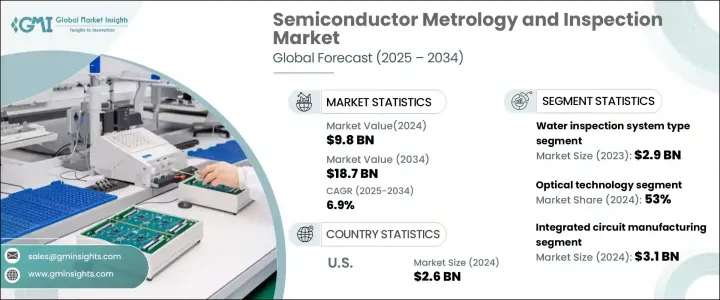
2024 年全球半導體計量和檢測市場價值為 98 億美元,預計 2025 年至 2034 年期間的複合年成長率為 6.9%。半導體製造流程的快速發展,加上對高性能晶片日益成長的需求,正在推動市場向前發展。隨著晶片設計變得越來越複雜,電晶體尺寸越來越小,製造商在確保精度和可靠性方面面臨越來越大的挑戰。這導致對能夠以奈米級精度檢測缺陷的先進計量和檢測系統的需求增加。汽車、消費性電子和電信等產業嚴重依賴這些解決方案來維持高生產良率並最大限度地減少製造過程中代價高昂的錯誤。
全球對半導體製造業的投資激增,特別是為應對供應鏈中斷和地緣政治因素,正在推動市場成長。世界各國政府和私人企業正在擴大半導體製造設施,迫切需要精確的計量和檢測系統。人工智慧、物聯網和 5G 技術的興起進一步擴大了對半導體元件的需求,因此需要採取嚴格的品質控制措施。此外,隨著產業轉向採用極紫外線 (EUV) 微影技術進行先進晶片生產,對能夠在原子尺度上進行測量的計量工具的需求比以往任何時候都更加重要。
| 市場範圍 | |
|---|---|
| 起始年份 | 2024 |
| 預測年份 | 2025-2034 |
| 起始值 | 98億美元 |
| 預測值 | 187億美元 |
| 複合年成長率 | 6.9% |
半導體計量和檢測市場涵蓋多個類別,包括晶圓檢測系統、光罩檢測系統、凸塊檢測、薄膜計量和引線框架檢測。 2023年,晶圓檢測系統佔據了相當大的佔有率,價值達29億美元。這些系統在識別半導體晶圓上的物理和圖案缺陷方面發揮著至關重要的作用。透過捕捉精確的座標,製造商可以區分由污染物引起的隨機缺陷和與曝光或掩模條件相關的系統缺陷。高精度檢測缺陷的能力對於最佳化生產效率和提高半導體裝置的品質至關重要。
市場也根據技術進行細分,其中光學、電子束和其他先進技術處於領先地位。預計光學技術將在 2024 年佔據市場主導地位,佔據 53% 的佔有率。光學計量解決方案因其能夠以奈米精度測量和分析積體電路和半導體晶圓而被廣泛採用,可確保光刻過程中的正確對準。它們能夠捕捉微小缺陷,這使得它們在精度至關重要的現代半導體製造中不可或缺。
預計到 2034 年,德國半導體計量和檢測市場規模將達到 11 億美元。作為全球半導體供應鏈的關鍵參與者,德國繼續大力投資先進製造解決方案。該國在汽車、工業和消費性電子產業的領導地位正在推動對高精度計量工具的需求。隨著本地代工廠擴大業務,用於支援晶圓製造和先進封裝的複雜計量和檢測系統的需求預計將大幅增加。
目錄
第1章:方法論與範圍
- 市場範圍和定義
- 基礎估算與計算
- 預測計算
- 資料來源
- 基本的
- 次要
- 付費來源
- 公共資源
第2章:執行摘要
第3章:行業洞察
- 產業生態系統分析
- 影響價值鏈的因素
- 利潤率分析
- 中斷
- 未來展望
- 製造商
- 經銷商
- 供應商格局
- 利潤率分析
- 重要新聞和舉措
- 監管格局
- 衝擊力
- 成長動力
- 半導體裝置日益複雜
- 光刻技術的進步
- 消費性電子產品需求不斷成長
- 對物聯網和 5G 設備的需求不斷成長
- 增加對半導體製造的投資
- 產業陷阱與挑戰
- 先進設備成本高
- 與現有系統的整合問題
- 成長動力
- 成長潛力分析
- 波特的分析
- PESTEL分析
第4章:競爭格局
- 介紹
- 公司市佔率分析
- 競爭定位矩陣
- 戰略展望矩陣
第5章:市場估計與預測:依類型,2021-2034
- 主要趨勢
- 晶圓檢測系統
- 掩模檢測系統
- 薄膜計量
- 碰撞檢查
- 引線框架檢查
第6章:市場估計與預測:依技術,2021-2034 年
- 主要趨勢
- 光學的
- 電子束
- 其他
第7章:市場估計與預測:按應用,2021-2034
- 主要趨勢
- 積體電路製造
- 發光二極體 (LED) 製造
- 分立元件
- 包裝和組裝
- 其他
第8章:市場估計與預測:依最終用途,2021-2034
- 主要趨勢
- 半導體代工廠
- 整合設備製造商 (IDM)
- 第三方業務(OSAT)
- 研發機構
第9章:市場估計與預測:按地區,2021-2034
- 主要趨勢
- 北美洲
- 美國
- 加拿大
- 歐洲
- 英國
- 德國
- 法國
- 義大利
- 西班牙
- 俄羅斯
- 亞太地區
- 中國
- 印度
- 日本
- 韓國
- 澳洲
- 拉丁美洲
- 巴西
- 墨西哥
- MEA
- 南非
- 沙烏地阿拉伯
- 阿拉伯聯合大公國
第10章:公司簡介
- Advantest Corporation
- Applied Materials, Inc.
- ASML Holding NV
- Bruker Corporation
- Camtek Ltd.
- Hitachi Ltd.
- JEOL Ltd.
- KLA Corporation
- Lasertec Corporation
- Nikon Corporation
- Nova Measuring Instruments Ltd.
- Olympus (EVIDENT)
- Onto Innovation, Inc
- Park Systems Corp.
- Thermo Fisher Scientific Inc.
- Toray Engineering Co., Ltd.
- Zygo Corporation
The Global Semiconductor Metrology And Inspection Market was valued at USD 9.8 billion in 2024 and is projected to expand at a CAGR of 6.9% from 2025 to 2034. The rapid evolution of semiconductor manufacturing processes, coupled with the growing demand for high-performance chips, is driving the market forward. As chip designs become more complex and transistor sizes shrink, manufacturers face increasing challenges in ensuring precision and reliability. This has led to a heightened demand for advanced metrology and inspection systems that can detect defects at nanometer-scale accuracy. Industries such as automotive, consumer electronics, and telecommunications rely heavily on these solutions to maintain high production yields and minimize costly errors in fabrication.
A surge in global investments in semiconductor manufacturing, particularly in response to supply chain disruptions and geopolitical factors, is fueling market growth. Governments and private enterprises worldwide are expanding semiconductor fabrication facilities, creating a pressing need for precise metrology and inspection systems. The rise of AI, IoT, and 5G technologies further amplifies the demand for semiconductor components, necessitating stringent quality control measures. Additionally, as the industry shifts toward extreme ultraviolet (EUV) lithography for advanced chip production, the need for metrology tools capable of measuring at the atomic scale is more critical than ever.
| Market Scope | |
|---|---|
| Start Year | 2024 |
| Forecast Year | 2025-2034 |
| Start Value | $9.8 Billion |
| Forecast Value | $18.7 Billion |
| CAGR | 6.9% |
The semiconductor metrology and inspection market encompasses various categories, including wafer inspection systems, mask inspection systems, bump inspection, thin film metrology, and lead frame inspection. In 2023, wafer inspection systems accounted for a substantial share, valued at USD 2.9 billion. These systems play a crucial role in identifying both physical and pattern defects on semiconductor wafers. By capturing precise coordinates, manufacturers can differentiate between random defects caused by contaminants and systematic defects related to exposure or mask conditions. The ability to detect defects with high precision is essential for optimizing production efficiency and enhancing the quality of semiconductor devices.
The market is also segmented based on technology, with optical, E-beam, and other advanced technologies leading the space. Optical technology is anticipated to dominate the market in 2024, securing a 53% share. Widely adopted due to its ability to measure and analyze integrated circuits and semiconductor wafers with nanometer accuracy, optical metrology solutions ensure proper alignment during the lithography process. Their capability to capture minute defects makes them indispensable in modern semiconductor manufacturing, where precision is paramount.
Germany semiconductor metrology and inspection market is projected to reach USD 1.1 billion by 2034. As a key player in the global semiconductor supply chain, Germany continues to invest heavily in advanced manufacturing solutions. The country's leadership in automotive, industrial, and consumer electronics industries is fueling the demand for high-precision metrology tools. With local foundries expanding operations, the need for sophisticated metrology and inspection systems to support wafer fabrication and advanced packaging is expected to rise significantly.
Table of Contents
Chapter 1 Methodology & Scope
- 1.1 Market scope & definitions
- 1.2 Base estimates & calculations
- 1.3 Forecast calculations
- 1.4 Data sources
- 1.4.1 Primary
- 1.4.2 Secondary
- 1.4.2.1 Paid sources
- 1.4.2.2 Public sources
Chapter 2 Executive Summary
- 2.1 Industry synopsis, 2021-2034
Chapter 3 Industry Insights
- 3.1 Industry ecosystem analysis
- 3.1.1 Factor affecting the value chain
- 3.1.2 Profit margin analysis
- 3.1.3 Disruptions
- 3.1.4 Future outlook
- 3.1.5 Manufacturers
- 3.1.6 Distributors
- 3.2 Supplier landscape
- 3.3 Profit margin analysis
- 3.4 Key news & initiatives
- 3.5 Regulatory landscape
- 3.6 Impact forces
- 3.6.1 Growth drivers
- 3.6.1.1 Increasing complexity of semiconductor devices
- 3.6.1.2 Advancements in lithography technologies
- 3.6.1.3 Rising consumer electronics demand
- 3.6.1.4 Rising demand for IoT and 5G-enabled devices
- 3.6.1.5 Increased investment in semiconductor manufacturing
- 3.6.2 Industry pitfalls & challenges
- 3.6.2.1 High cost of advanced equipment
- 3.6.2.2 Integration issues with existing systems
- 3.6.1 Growth drivers
- 3.7 Growth potential analysis
- 3.8 Porter's analysis
- 3.9 PESTEL analysis
Chapter 4 Competitive Landscape, 2024
- 4.1 Introduction
- 4.2 Company market share analysis
- 4.3 Competitive positioning matrix
- 4.4 Strategic outlook matrix
Chapter 5 Market Estimates & Forecast, By Type, 2021-2034 (USD Million)
- 5.1 Key trends
- 5.2 Wafer inspection system
- 5.3 Mask inspection system
- 5.4 Thin film metrology
- 5.5 Bump inspection
- 5.6 Lead frame inspection
Chapter 6 Market Estimates & Forecast, By Technology, 2021-2034 (USD Million)
- 6.1 Key trends
- 6.2 Optical
- 6.3 E-beam
- 6.4 Others
Chapter 7 Market Estimates & Forecast, By Application, 2021-2034 (USD Million)
- 7.1 Key trends
- 7.2 Integrated circuit manufacturing
- 7.3 Light Emitting Diode (LED) manufacturing
- 7.4 Discrete devices
- 7.5 Packaging and assembly
- 7.6 Others
Chapter 8 Market Estimates & Forecast, By End Use, 2021-2034 (USD Million)
- 8.1 Key trends
- 8.2 Semiconductor foundries
- 8.3 Integrated Device Manufacturers (IDMs)
- 8.4 Third-Party Business (OSAT)
- 8.5 Research & Development (R&D) institutions
Chapter 9 Market Estimates & Forecast, By Region, 2021-2034 (USD Million)
- 9.1 Key trends
- 9.2 North America
- 9.2.1 U.S.
- 9.2.2 Canada
- 9.3 Europe
- 9.3.1 UK
- 9.3.2 Germany
- 9.3.3 France
- 9.3.4 Italy
- 9.3.5 Spain
- 9.3.6 Russia
- 9.4 Asia Pacific
- 9.4.1 China
- 9.4.2 India
- 9.4.3 Japan
- 9.4.4 South Korea
- 9.4.5 Australia
- 9.5 Latin America
- 9.5.1 Brazil
- 9.5.2 Mexico
- 9.6 MEA
- 9.6.1 South Africa
- 9.6.2 Saudi Arabia
- 9.6.3 UAE
Chapter 10 Company Profiles
- 10.1 Advantest Corporation
- 10.2 Applied Materials, Inc.
- 10.3 ASML Holding N.V
- 10.4 Bruker Corporation
- 10.5 Camtek Ltd.
- 10.6 Hitachi Ltd.
- 10.7 JEOL Ltd.
- 10.8 KLA Corporation
- 10.9 Lasertec Corporation
- 10.10 Nikon Corporation
- 10.11 Nova Measuring Instruments Ltd.
- 10.12 Olympus (EVIDENT)
- 10.13 Onto Innovation, Inc
- 10.14 Park Systems Corp.
- 10.15 Thermo Fisher Scientific Inc.
- 10.16 Toray Engineering Co., Ltd.
- 10.17 Zygo Corporation
 曲線追蹤器市場報告:趨勢、預測和競爭分析(至 2031 年)
 半導體計量和測試市場按類型、技術類型、組件類型、最終用戶、應用和行業細分 - 2025-2030 年全球預測
 2025 年全球半導體計量和測試市場報告
 半導體測量與檢測設備:市場佔有率分析、產業趨勢、成長預測(2024-2029)半導體計量和檢測系統市場,依類型、技術、組織規模、應用、國家和地區 - 2024-2032 年行業分析、市場規模、市場佔有率和預測
 半導體測量·檢驗的全球市場 - 主要趨勢與機會(~2029年)半導體計量設備市場 - 2023-2031年全球行業分析、規模、佔有率、成長、趨勢和預測