


 |
市場調查報告書
商品編碼
1479764
薄膜形成:趨勢、關鍵問題與市場分析Thin Film Deposition: Trends, Key Issues, Market Analysis |
||||||
簡介
在半導體工業中,薄膜形成在電子元件的製造過程中發揮重要作用,它提供了在半導體基板上形成精確且受控的材料薄層的方法。 幾個值得注意的趨勢正在塑造半導體薄膜形成市場,反映了技術進步、不斷變化的行業要求和新應用。
首先,對提供高產量、均勻性和可擴展性的薄膜形成技術的需求不斷增長。 隨著半導體裝置變得越來越複雜和集成,製造商需要能夠擴展到更大的基板尺寸並在整個表面積上實現一致的薄膜特性的沉積方法。 這一趨勢正在推動原子層沉積 (ALD) 和化學氣相沉積 (CVD) 等創新薄膜沉積製程的發展,這些製程可實現大批量生產,同時可以精確控制薄膜厚度和成分。
半導體薄膜形成市場的另一個趨勢是越來越多地採用先進材料進行薄膜形成。 隨著裝置性能要求的不斷提高,對具有導電性、光學透明度和熱穩定性等客製化特性的薄膜的需求不斷增長。 這一趨勢正在推動專注於探索新材料的研發工作,以滿足下一代電子設備不斷變化的需求。
此外,人們對支援三維 (3D) 半導體結構和異構整合平台製造的薄膜形成技術越來越感興趣。 隨著 3D IC 和系統單晶片 (SoC) 架構等技術的出現,對能夠在非平面表面上形成薄膜並實現精確的層間對準的沉積方法的需求不斷增長。
此外,有一種趨勢是將薄膜形成技術與原位監測和控制功能相結合,從而實現即時製程優化和缺陷檢測。 透過將先進的計量工具和回饋機制整合到沉積系統中,製造商可以提高製程穩定性、產量和可重複性,並降低半導體設備的生產成本和上市時間。
總體而言,半導體薄膜形成市場的趨勢凸顯了該行業對創新解決方案的持續探索,以實現具有卓越性能、功能和可靠性的先進電子設備的生產。 隨著半導體技術的不斷發展,薄膜形成仍然是推動半導體產業進步和創新的關鍵技術。
薄膜沉積技術的趨勢
半導體薄膜形成技術的趨勢特徵是精度更高、材料多樣性、設備複雜性、環境永續性和製程智慧化。 這些趨勢正在塑造新沉積方法和材料的發展,推動半導體產業朝向具有前所未有的性能和功能的下一代電子產品發展。
由於電子元件不斷追求小型化、性能提高和成本效率,半導體薄膜形成技術的情況正在發生重大變化。 這種演變的特點是幾個重要趨勢,反映了半導體產業不斷變化的需求以及旨在滿足這些需求的技術創新。
原子層沉積 (ALD) 等技術越來越受到關注,因為它們可以一次沉積一個原子層,從而可以對薄膜厚度和成分進行無與倫比的控制。 這種精度對於製造下一代半導體設備至關重要,即使很小的偏差也會對設備性能產生重大影響。 ALD 保形沉積複雜 3D 結構的能力對於 3D 積體電路 (IC) 和先進儲存技術等先進應用至關重要。
傳統的矽基半導體正在被各種新材料增強或取代,例如高 k 電介質、金屬氧化物以及石墨烯和過渡金屬二硫屬化物等二維 (2D) 材料。 這些材料具有優異的電氣、熱和機械性能,有助於開發更高性能和更低功耗的設備。 結合這些材料需要沉積技術的進步,以解決其獨特的性能和整合課題。
本報告研究和分析了全球半導體市場,並對薄膜沉積技術的現狀進行了展望。 它還確定了研究重點、等待解決的技術課題以及預期的市場變化。
目錄
第一章簡介
第 2 章執行摘要
第 3 章物理氣相沉積
- 簡介
- 濺鍍技術
- 等離子技術
- 反應器設計
- 半導體工藝
- 目標
第 4 章化學氣相沉積
- 簡介
- 化學氣相沉積(CVD)技術
- APCVD
- LPCVD
- 等離子CVD
- HDPCVD
- 阿爾達
第五章電化學沉積
- 簡介
- 反應器設計
- 作業
- 添加劑
- 處理中
- 銅陰極
- 濕銅種子層
第六章成膜與薄膜特性
- 簡介
- 介電膜形成
- 金屬沉積
第 7 章供應商問題
- 簡介
- 450mm加工
- 整合處理
- 銅
- 測量
- 靜電放電
- 參數測試
第八章市場預測
- 簡介
- 主要問題
- 市場預測的假設
- 市場預測
- 化學氣相沉積
- 物理氣相沉積
- 電鍍銅市場
- ALD 市場
Introduction
In the semiconductor industry, thin film deposition plays a crucial role in the manufacturing process of electronic devices, providing a method to deposit thin layers of materials onto semiconductor substrates with precision and control. Several notable trends are shaping the semiconductor thin film deposition markets, reflecting advancements in technology, evolving industry requirements, and emerging applications.
Firstly, there is a growing demand for thin film deposition techniques that offer high throughput, uniformity, and scalability. As semiconductor devices become increasingly complex and integrated, manufacturers require deposition methods that can accommodate larger substrate sizes and deliver consistent film properties across the entire surface area. This trend is driving the development of innovative deposition processes, such as atomic layer deposition (ALD) and chemical vapor deposition (CVD), which offer precise control over film thickness and composition while enabling high-volume production.
Another trend in the semiconductor thin film deposition markets is the increasing adoption of advanced materials for thin film deposition. As device performance requirements continue to escalate, there is a growing need for thin films with tailored properties, such as enhanced electrical conductivity, optical transparency, and thermal stability. This trend is driving research and development efforts focused on exploring new materials to meet the evolving demands of next-generation electronic devices.
Furthermore, there is a rising emphasis on thin film deposition techniques that support the fabrication of three-dimensional (3D) semiconductor structures and heterogeneous integration platforms. With the advent of technologies like 3D ICs and system-on-chip (SoC) architectures, there is a growing need for deposition methods capable of depositing thin films on non-planar surfaces and achieving precise layer-to-layer alignment.
Moreover, there is a trend towards the integration of thin film deposition techniques with insitu monitoring and control capabilities, enabling real-time process optimization and defect detection. By incorporating advanced metrology tools and feedback mechanisms into deposition systems, manufacturers can enhance process stability, yield, and reproducibility, thereby reducing production costs and time-to-market for semiconductor devices.
Overall, the trends in the semiconductor thin film deposition markets underscore the industry's ongoing quest for innovative solutions that enable the fabrication of advanced electronic devices with superior performance, functionality, and reliability. As semiconductor technologies continue to evolve, thin film deposition will remain a critical enabling technology, driving progress and innovation in the semiconductor industry.
Trends in Deposition Technology
The trends in semiconductor thin film deposition technology are characterized by a move towards greater precision, material diversity, device complexity, environmental sustainability, and process intelligence. These trends are shaping the development of new deposition methods and materials, driving the semiconductor industry towards the next generation of electronic devices with unprecedented performance and functionality.
The landscape of semiconductor thin film deposition technology is undergoing significant transformation, driven by the relentless pursuit of miniaturization, enhanced performance, and cost-efficiency in electronic devices. This evolution is marked by several key trends that reflect the changing demands of the semiconductor industry and the technological innovations designed to meet these needs.
A pivotal trend is the shift towards atomic precision in thin film deposition processes. Techniques such as Atomic Layer Deposition (ALD) are gaining prominence for their ability to deposit films one atomic layer at a time, offering unparalleled control over film thickness and composition. This precision is crucial for manufacturing the next generation of semiconductor devices, where even minor deviations can significantly impact device performance. ALD's ability to conformally coat complex 3D structures makes it indispensable for advanced applications, including 3D integrated circuits (ICs) and advanced memory technologies.
Another significant trend is the diversification of materials used in thin film deposition. Traditional silicon-based semiconductors are being augmented or replaced by a variety of new materials, including high-k dielectrics, metal oxides, and two-dimensional (2D) materials like graphene and transition metal dichalcogenides. These materials offer superior electrical, thermal, and mechanical properties, enabling the development of devices with higher performance and lower power consumption. The incorporation of these materials necessitates advancements in deposition technologies that can handle their unique properties and integration challenges.
The push for greater device integration and functionality is driving the adoption of complex multi-layer structures, which require sophisticated deposition techniques capable of delivering high-quality films with strict interlayer interfaces and uniformity. As devices shrink and the number of layers increases, deposition technologies must offer excellent control over interface engineering, stress management, and layer uniformity to ensure device reliability and performance.
Environmental sustainability and energy efficiency are also becoming critical considerations in thin film deposition processes. The semiconductor industry is increasingly focused on reducing the environmental footprint of manufacturing processes, leading to the development of deposition techniques that consume less energy, use fewer hazardous chemicals, and generate less waste. This trend is not only driven by regulatory pressures but also by the industry's recognition of the importance of sustainable practices for long-term viability.
Lastly, the integration of in-situ monitoring and analytics with deposition processes is a growing trend. Advanced sensors and data analytics are being incorporated directly into deposition systems, enabling real-time process control and optimization. This integration enhances process repeatability, improves yield, and reduces the need for post-deposition inspection, thereby lowering manufacturing costs and improving device performance.
The Need for This Report
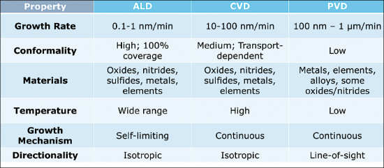
This comprehensive semiconductor deposition report provides an in-depth exploration into the multifaceted domain of deposition technologies pivotal to semiconductor manufacturing. It begins with a foundational overview of thin film deposition, shedding light on critical processes such as physical vapor deposition (PVD), chemical vapor deposition (CVD), atomic layer deposition (ALD), and molecular beam epitaxy (MBE). This section demystifies the principles behind each method, offering a comparative analysis to aid in understanding their unique benefits, limitations, and suitability for various semiconductor applications.
Delving into market dynamics, the report presents a detailed examination of global and regional trends, highlighting market growth, demand patterns, and future projections. It paints a comprehensive picture of the competitive landscape, identifying key players, their market positioning, strategic initiatives, and technological breakthroughs. Furthermore, it discusses the impact of regulatory frameworks and environmental standards on deposition practices, emphasizing the industry's response to sustainability and safety mandates.
Technological advancements occupy a central role in the report, showcasing the latest innovations that enhance film quality, deposition efficiency, and material diversity. It highlights the advent of new materials like 2D materials, high-k dielectrics, and metal oxides that promise to revolutionize semiconductor device performance. The narrative extends to the challenges of integrating these advanced deposition processes into mainstream manufacturing, addressing scalability, quality control, and cost-effectiveness.
The application of deposition technologies in fabricating cutting-edge electronic devices is thoroughly analyzed. This includes their role in developing logic chips, memory devices, power electronics, and their contribution to emerging sectors like 3D integrated circuits (ICs), flexible electronics, and solar cells. The report ventures into the future, speculating on the direction of research and development efforts aimed at overcoming existing technological hurdles, enhancing process capabilities, and discovering environmentally friendly deposition methods.
In its concluding sections, the report provides a forward-looking perspective on the deposition technology landscape, identifying research priorities, technological challenges awaiting resolution, and anticipated market shifts. It features case studies and expert opinions to ground its predictions in real-world examples and authoritative insights, offering readers a wellrounded understanding of the current state and future potential of semiconductor deposition technologies.
By weaving together these diverse strands of information, the report serves as a valuable resource for stakeholders across the semiconductor industry spectrum, from manufacturers and researchers to policymakers and investors, equipping them with the knowledge to navigate the complexities of semiconductor deposition in an era of rapid technological change.
About this Report
Thin film deposition processes play a critical role in the production of high-density, highperformance microelectronic products. Considerable progress has been achieved in the development of deposition processes -- and in the development of the reactor systems in which they are carried out. This report discusses relevant mechanisms; processing, system, and materials aspects, potential advances, and considerations regarding extendibility to a wafer diameter of 300 mm and beyond.
With the introduction of new thin-film materials to consistently shrinking microelectronic devices and circuits, and as the aperture ratio of an integrated-circuit structure increases, conformal step coverage becomes increasingly difficult to achieve. This report compares some of the issues impacting users of different deposition tools, including:
|
|
|
In addition, as device geometries shrink, semiconductor manufacturing has become increasingly complex and precise, requiring a better understanding of the specific processes involved. These issues are described in the report.
This report discusses the technology trends, products, applications, and suppliers of materials and equipment. It also gives insights to suppliers for future user needs and should assist them in long range planning, new product development and product improvement. A market forecast for Thin Film Deposition Tools is presented including market shares by deposition type between 2012 and 2023.
Table of Contents
Chapter 1. Introduction
Chapter 2. Executive Summary
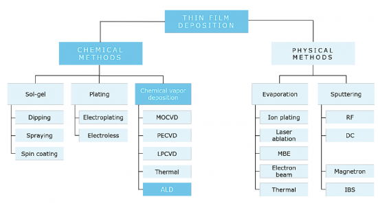
Chapter 3. Physical Vapor Deposition
- 3.1. Introduction
- 3.2. Sputtering Technology
- 3.3. Plasma Technology
- 3.4. Reactor Designs
- 3.4.1. Long-Throw Deposition
- 3.4.2. Collimated Sputter Deposition
- 3.4.3. Showerhead Deposition
- 3.4.4. Ionized PVD
- 3.5. Semiconductor Processing
- 3.5.1. Feature Patterning
- 3.5.2. Gap Fill
- 3.6. Targets
Chapter 4. Chemical Vapor Deposition
- 4.1. Introduction
- 4.2. Chemical Vapor Deposition (CVD) Techniques
- 4.2.1. APCVD
- 4.2.2. LPCVD
- 4.2.3. PECVD
- 4.2.4. HDPCVD
- 4.2.5. ALD
Chapter 5. Electrochemical Deposition
- 5.1. Introduction
- 5.2. Reactor Design
- 5.3. Challenges
- 5.4. Additives
- 5.5. Processing
- 5.5.1. Superfilling
- 5.5.2. Aspect Ratios
- 5.6. Copper Cathodes
- 5.7. Wet Copper Seed-Layer
Chapter 6. Film Deposition And Film Properties
- 6.1. Introduction
- 6.2. Dielectric Deposition
- 6.2.1. Silicon Dioxide
- 6.2.1.1. Thermal CVD
- 6.2.1.2. PECVD
- 6.2.1.3. HDPCVD
- 6.2.2. Silicon Nitride
- 6.2.2.1. Thermal CVD
- 6.2.2.2. PECVD
- 6.2.2.3. HDPCVD
- 6.2.3. High-K Dielectrics
- 6.2.4. Low-K Dielectrics
- 6.2.1. Silicon Dioxide
- 6.3. Metal Deposition
- 6.3.1. Aluminum
- 6.3.2. Tungsten/Tungsten Silicide
- 6.3.3. Titanium Nitride
Chapter 7. Vendor Issues
- 7.1. Introduction
- 7.2 450mm Processing
- 7.3. Integrated Processing
- 7.4. Copper
- 7.5. Metrology
- 7.6. ESD
- 7.7. Parametric Test
Chapter 8. Market Forecast
- 8.1. Introduction
- 8.2. Key Issues
- 8.3. Market Forecast Assumptions
- 8.4. Market Forecast
- 8.4.1. Chemical Vapor Deposition
- 8.4.2. Physical Vapor Deposition
- 8.4.3. Copper Electroplating Market
- 8.4.4. Atomic Layer Deposition Market
List of Figures
- 3.1. Schematic Of Sputtering System
- 3.2. Magnetron Sputtering Design
- 3.3. Showerhead Reactor Design
- 3.4. Ionized PVD
- 4.1. APCVD Reactor
- 4.2. Tube CVD Reactor
- 4.3. HDPCVD Reactor
- 4.4. ALD Versus PVD Copper Barrier
- 5.1. Copper Electroplating System
- 7.1. Comparison Between Semiconductor and Equipment Revenues
- 8.1. Worldwide MCVD Market Shares
- 8.2. Worldwide DCVD Market Shares
- 8.3. Worldwide DCVD Market By Sectors
- 8.4. Worldwide HDHCVD Market Shares
- 8.5. Worldwide PECVD Market Shares
- 8.6. Worldwide SACVD Market Shares
- 8.7. Worldwide LPCVD Market Shares
- 8.8. Worldwide PVD Market Shares
- 8.9. Worldwide ECD Market Shares
- 8.10. Worldwide ALD Market Shares
List of Tables
- 8.1. Worldwide CVD Market Forecast
- 8.2. Worldwide MCVD Market Shares
- 8.3. Worldwide DCVD Market Shares
- 8.4. Worldwide HDPCVD Market Forecast
- 8.5. Worldwide HDPCVD Market Shares
- 8.6. Worldwide PECVD Market Forecast
- 8.7. Worldwide PECVD Market Shares
- 8.8. Worldwide SACVD Market Forecast
- 8.9. Worldwide SACVD Market Shares
- 8.10. Worldwide LPCVD Market Forecast
- 8.11. Worldwide LPCVD Market Shares
- 8.12. Worldwide PVD Market Forecast
- 8.13. Worldwide PVD Market Shares
- 8.14. Worldwide ECD Market Forecast
- 8.15. Worldwide ALD Market Forecast
 離子布植設備市場:依晶圓尺寸、產品類型、能量範圍、離子源類型和最終用途產業分類-全球預測,2026-2032年
 薄膜沉積設備市場-2025-2030年預測外延沉積市場:預測(2025-2030 年)
 薄膜半導體沉積:全球市場佔有率和排名、總收入和需求預測(2025-2031年)按技術類型、設備類型、最終用途、材料類型、系統配置和壓力條件沉澱設備市場—2025-2032年全球預測
 薄膜半導體沉積市場機會、成長動力、產業趨勢分析與預測 2024 - 2032薄層累積設備的全球市場規模:各產品,各用途,各地區,範圍及預測
 氣相沉積市場:市場規模和佔有率分析 - 依製程、依應用、依最終用戶 - 收入估算和需求預測(截至 2030 年)