


 |
市場調查報告書
商品編碼
1550010
化學機械拋光 (CMP)墊片:市場佔有率分析、行業趨勢、成長預測(2024-2029 年)Chemical Mechanical Polishing (CMP) Pad - Market Share Analysis, Industry Trends & Statistics, Growth Forecasts (2024 - 2029) |
||||||
※ 本網頁內容可能與最新版本有所差異。詳細情況請與我們聯繫。
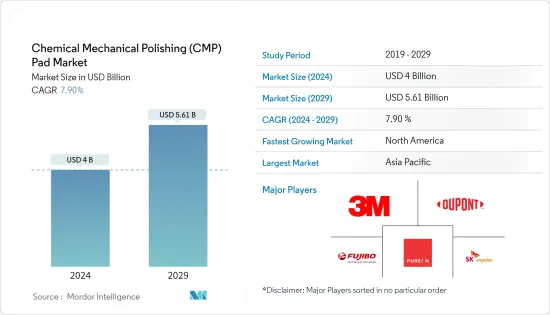
化學機械拋光(CMP)墊片市場規模預計到 2024 年為 40 億美元,預計到 2029 年將達到 56.1 億美元,預測期內(2024-2029 年)複合年成長率為 7.90%。
主要亮點
- 化學機械拋光是半導體晶圓製造過程中的關鍵步驟。在此過程中,晶圓的頂面被拋光以形成完美平坦的表面。這對於將化學漿料與機械運動相結合以創造更堅固耐用的半導體材料至關重要。
- 隨著電子設備性能標準的提高,半導體和電子設備需要更小、更耐用。因此,對 CMP 等先進製造材料和技術的需求不斷增加。對電子產品不斷成長的需求正在推動電子封裝行業的發展,客戶期望新電子設備具有增強的功能。
- 半導體產業是化學機械拋光墊片的重要消費者,特別是在半導體製造過程中的晶圓拋光過程中。在汽車電子、智慧型手機、物聯網設備和人工智慧 (AI) 技術等應用的推動下,對半導體的需求不斷成長,從而推動了對化學機械拋光墊片的需求。此外,半導體製造技術的不斷進步(例如小型化)正在推動對更精確、更有效率的 CMP墊片的需求。
- 3DE IC、穿透矽通孔(TSV) 和扇出晶圓級封裝 (FOWLP) 等封裝技術的日益普及需要先進的 CMP 拋光和表面處理解決方案。化學機械拋光 (CMP)墊片對於實現這些先進封裝製程所需的拋光、表面粗糙度和缺陷水平至關重要。
- 儘管化學機械拋光 (CMP)墊片材料和製造過程取得了進步,但某些技術限制仍然存在。這些限制包括實現超光滑表面、抑製表面下損傷、最小化邊緣效應以及解決墊片磨損和漿料消費量問題。可能需要進一步的研究和開發來克服這些限制,這是阻礙市場成長的一個因素。此外,CMP墊片製造商可能面臨與供應鏈中斷相關的風險,影響其滿足需求的能力。
- 技術進步、材料科學創新和製程工程發展等宏觀經濟因素正在為 CMP墊片製造商帶來挑戰和機會。解決與 CMP 製程控制、減少缺陷、材料相容性和表面品質改進相關的技術問題正在推動 CMP墊片市場的研發投資和產品創新。相反,CMP墊片材料、配方和製造技術的突破可以為創新供應商創造競爭優勢和市場機會。
化學機械拋光(CMP)墊片市場趨勢
300mm晶圓尺寸將大幅成長
- 在半導體產業,由於先進的製造程序,晶圓尺寸幾乎已經標準化在300mm左右。這種標準化簡化了供應鏈物流,並促進了半導體製造商、設備供應商和材料供應商之間的協作。因此,化學機械拋光 (CMP)墊片製造商正在優先開發和生產專為 300 mm 晶圓加工設計的 CMP墊片,以滿足產業需求。
- 全球300毫米晶圓廠產能擴張步伐正在放緩。然而,該行業仍專注於提高產能,以滿足強勁而穩定的半導體需求。例如,印度計劃於 2024 年 3 月開始生產半導體製造設備,應用材料公司率先在班加羅爾建立了驗證中心。我們在300mm晶圓加工方面也取得了進展,並在建立工程中心的同時致力於建立生態系統。這些技術創新正在推動研究目標市場的成長。
- 2023 年 11 月,德克薩斯(TI) 在華盛頓州李海市推出了名為 LFAB2 的新型 300 毫米半導體晶圓製造廠。 LFAB2 的建設將連接到該公司在該地點現有的 300 毫米晶圓廠。一旦完成,LFAB2 將使 TI 猶他工廠能夠每天滿載生產數千萬個嵌入式和類比處理晶片。 LFAB2 的目標是完全依靠可再生電力運行,在李海安裝 300mm 先進設備和製程將有助於最大限度地減少廢棄物、水和能源的使用。
- 晶圓尺寸向 300mm 的轉變通常與採用先進的半導體製造技術和縮小製程節點(7nm 和 5nm)有關。這些先進的節點技術需要更嚴格的製程控制和增強的拋光,以滿足嚴格的性能和可靠性要求。
- 化學機械拋光 (CMP)墊片的需求量很大,因為它們在實現先進節點製造所需的奈米級平坦度方面發揮關鍵作用。
亞太地區佔主要市場佔有率
- 亞太地區是世界半導體製造中心,中國、台灣、韓國、日本等國家在半導體製造領域扮演重要角色。該地區半導體製造業的成長推動了對晶圓拋光製程中使用的化學機械拋光 (CMP)墊片的強勁需求。
- 亞太地區處於技術進步的前沿,包括先進封裝技術、高效能運算和人工智慧(AI)的發展。這些進步需要精確、高效的 CMP 工藝,從而推動了對 CMP墊片的需求。
- 該地區繼續投資新的半導體製造設施(晶圓廠)並擴大現有設施。工廠產能的增加和先進製造設備的引進正在推動CMP墊片消費量的增加。例如,2024年3月,塔塔電子私人有限公司(TEPL)與台灣力晶半導體製造公司(PSMC)合作,在古吉拉突邦Dholera設立半導體工廠。該計劃投資額為9.1兆印度盧比(1,097.1億美元)。 PSMC 目前在台灣經營六家半導體代工廠。
- 新晶圓廠的產能將達到每月 50,000 片晶圓。 PSMC將專注於使用28奈米技術生產高性能運算和電源管理晶片,用於電動車、電訊、國防、汽車、消費性電子、顯示器和電力電子等各個產業。
- 在可支配收入增加、都市化和技術採用的推動下,亞太地區消費性電子市場正在經歷顯著擴張。對智慧型手機、筆記型電腦和電子設備的需求正在增加對半導體元件和 CMP墊片的需求。
- 此外,印度、越南和印尼等亞太地區的新興經濟體在各領域也擴大採用半導體技術。這些國家的工業化和數位化正在取得進展,半導體製造對 CMP墊片的需求預計將大幅成長。
- 智慧城市、5G網路和物聯網等正在進行的基礎設施開發計劃正在推動對半導體晶片和電子元件的需求。化學機械拋光 (CMP)墊片在生產這些基礎設施計劃所需的先進半導體元件方面發揮關鍵作用。
- 此外,亞太地區的政府和產業正在投資半導體研發以促進創新。旨在開發下一代材料、設備和製程的研究舉措正在促進對 CMP墊片的需求。
化學機械拋光 (CMP)墊片產業概覽
化學機械拋光(CMP)墊片市場競爭非常激烈。公司種類繁多,從大到小,所以非常集中。所有主要公司都佔有重要的市場佔有率,並致力於擴大其全球消費群。該市場的重要參與者包括 3M、杜邦、富士紡控股、Purion 和 SK Anpulse。為了在預測期內獲得競爭優勢,多家公司正在透過結盟、合作、收購和推出創新新產品來擴大市場佔有率。
- 2024年4月,決定SK海力士繼續在韓國的投資計畫。該公司正準備投資120兆日圓(7,400億美元)在龍仁半導體叢集建設生產設施。第一家工廠預計將於 2025 年 3 月開始建設,並於 2027 年初竣工。還將建造一座小型晶圓廠,使用 300 毫米晶圓加工設備來測試半導體材料、組件和設備。
- 2023年9月,SK Empulse出售了半導體基礎材料業務,濕化學業務被當地半導體/顯示材料公司Yaker Technology收購,清洗業務被投資公司Sunyang Shinjin收購。今年早些時候,SKC將其半導體材料和零件業務整合到SK Empulse,擴大了其在半導體前端工藝的高付加材料業務中的影響力,例如化學機械拋光(CMP)墊片和空白掩模。
其他好處:
- Excel 格式的市場預測 (ME) 表
- 3 個月分析師支持
目錄
第1章簡介
- 研究假設和市場定義
- 調查範圍
第2章調查方法
第3章執行摘要
第4章市場洞察
- 市場概況
- 產業吸引力-波特五力分析
- 新進入者的威脅
- 買家/消費者的議價能力
- 供應商的議價能力
- 替代品的威脅
- 競爭公司之間的敵對關係
- 技術簡介
- COVID-19 和其他宏觀經濟因素對市場的影響
第5章市場動態
- 市場促進因素
- 對複雜、高性能晶片/先進技術的需求不斷成長
- 小節點與新架構簡介
- 市場限制因素
- 半導體產業的週期性和動態性
第6章 市場細分
- 按晶圓尺寸
- 300 mm
- 200 mm
- 其他晶圓尺寸
- 按地區
- 北美洲
- 歐洲
- 中國
- 韓國
- 日本
- 台灣
第7章 競爭格局
- 公司簡介
- 3M Co.
- DuPont de Nemours Inc.
- Fujibo Holdings Inc.
- Pureon
- SK enpulse
- Thomas West Inc.
- Hubei DingLong
- Cabot Corporation
- Entegris
- Beijing Grish Hitech Co. Ltd
第8章投資分析
第9章市場的未來
The Chemical Mechanical Polishing Pad Market size is estimated at USD 4 billion in 2024, and is expected to reach USD 5.61 billion by 2029, growing at a CAGR of 7.90% during the forecast period (2024-2029).
Key Highlights
- Chemical mechanical polishing is a crucial step in the semiconductor wafer manufacturing process. During this process, the top surface of the wafer is polished to create a completely flat surface, which is essential for building more robust and durable semiconductor materials using a combination of chemical slurry and mechanical movements.
- The rising performance standards of electronic devices are leading to a need for smaller and more durable semiconductors and electronic devices. This, in turn, increases the requirement for advanced fabrication materials and techniques such as CMP. The growing demand for electronic products drives the electronic packaging industry, with customers expecting enhanced features in new electronic devices.
- The semiconductor industry is a significant consumer of chemical mechanical polishing pads, particularly for wafer polishing processes during semiconductor manufacturing. The increasing demand for semiconductors driven by applications such as automotive electronics, smartphones, IoT devices, and AI (artificial intelligence) technologies fuels the demand for chemical mechanical polishing pads. Moreover, the continuous technological advancements in semiconductor fabrication technologies, including the development of smaller feature sizes, drive the need for more precise and efficient CMP pads.
- The rising adoption of packaging technologies such as 3DE ICs, through-silicon vias(TSVs), and fan-out wafer-level packaging (FOWLP) necessitates advanced CMP polishing and surface preparation solutions. Chemical mechanical polishing (CMP) pads are crucial in achieving the required polishing, surface roughness, and defectivity levels of these advanced packaging processes.
- Despite the advancements in chemical mechanical polishing (CMP) pad materials and manufacturing processes, certain technological limitations persist. These limitations include achieving ultra-smooth surfaces, controlling sub-surface damage, minimizing edge effects, and addressing pad wear and slurry consumption issues. Overcoming these limitations may require further research and development efforts, thus hindering the market's growth. Moreover, CMP pad manufacturers may face risks associated with supply chain disruptions, impacting the ability to meet demand.
- Macroeconomic factors such as technological advancements, material science innovations, and process engineering developments are presenting challenges and opportunities for CMP pad manufacturers. Addressing technical difficulties related to CMP process control, defect reduction, material compatibility, and surface quality improvement drives R&D investments and product innovation in the CMP pads market. Conversely, breakthroughs in CMP pad materials, formulations, or manufacturing techniques can create competitive advantages and market opportunities for innovative suppliers.
Chemical Mechanical Polishing (CMP) Pad Market Trends
300 mm Wafer Size to Witness a Significant Growth
- The semiconductor industry has largely standardized around 300 mm wafer size for advanced manufacturing processes. This standardization simplifies supply chain logistics and facilitates collaboration among semiconductor manufacturers, equipment suppliers, and materials providers. As a result, chemical mechanical polishing (CMP) pad manufacturers prioritize developing and producing CMP pads designed for 300 mm wafer processing to meet the industry demand.
- The rate of global 300 mm fab capacity expansion is slowing down. However, the industry is still dedicated to increasing capacity to keep up with the firm and consistent semiconductor demand. For instance, in March 2024, India planned to produce equipment for semiconductor manufacturing, with Applied Materials taking the lead by establishing a validation center in Bengaluru. The country is also advancing in 300 mm wafer processing and is focusing on creating a supportive ecosystem while establishing an engineering center. These innovations are driving the growth of the market studied.
- In November 2023, Texas Instruments launched a new 300 mm semiconductor wafer fabrication plant called LFAB2 in Lehi, Utah. The construction of LFAB2 will be connected to the company's existing 300 mm wafer fab in the exact location. Once LFAB2 is finished, both of TI's Utah fabs will be capable of producing tens of millions of embedded and analog processing chips daily at maximum capacity. LFAB2 aims to operate solely on renewable electricity, and the implementation of advanced 300 mm equipment and processes in Lehi will help minimize waste, water, and energy usage.
- The shift to 300 mm wafer size is often associated with adopting advanced semiconductor manufacturing technologies and smaller process nodes (7 nm and 5 nm). These advanced node technologies require tighter process control and enhanced polishing to meet stringent performance and reliability requirements.
- Chemical mechanical polishing (CMP) pads are in high demand because they play a crucial role in achieving the nanoscale-level planarity required for advanced node fabrication.
Asia-Pacific to Hold Significant Market Share
- Asia-Pacific is a global semiconductor manufacturing hub, with countries like China, Taiwan, South Korea, and Japan playing significant roles in semiconductor fabrication. The region's growth in semiconductor manufacturing drives the substantial demand for chemical mechanical polishing (CMP) pads used in wafer polishing processes.
- Asia-Pacific is at the forefront of technological advancements, including developing advanced packaging technologies, high-performance computing, and AI (artificial intelligence). These advancements require precise and efficient CMP processes, boosting the demand for CMP pads.
- The region continues to witness investments in new semiconductor fabrication facilities (fabs) and the expansion of existing ones. Increasing fab capacity and installing advanced manufacturing equipment contribute to the higher consumption of CMP pads. For instance, in March 2024, Tata Electronics Private Limited (TEPL) partnered with Taiwan's Powerchip Semiconductor Manufacturing Corp. (PSMC) to set up a semiconductor fab in Dholera, Gujarat. The investment for this project is INR 9,100 billion (USD 109.71 billion). PSMC currently operates six semiconductor foundries in Taiwan.
- The capacity of the new fabs will be 50,000 wafer starts per month. PSMC will focus on producing high-performance compute chips using 28 nm technology and power management chips for various industries such as electric vehicles, telecom, defense, automotive, consumer electronics, display, and power electronics.
- Asia-Pacific is home to a large and expanding consumer electronics market driven by rising disposable incomes, urbanization, and technological proliferation. The demand for smartphones, laptops, and electronic devices fuels the need for semiconductor components and CMP pads.
- Moreover, emerging economies in Asia-Pacific, such as India, Vietnam, and Indonesia, are witnessing increasing adoption of semiconductor technologies across various sectors. As these economies continue to industrialize and digitize, the demand for CMP pads for semiconductor manufacturing is expected to grow significantly.
- Ongoing infrastructure development projects, such as smart cities, 5G networks, and the IoT, drive demand for semiconductor chips and electronic components. The chemical mechanical polishing (CMP) pads play a significant role in enabling the production of advanced semiconductor devices required for these infrastructure projects.
- In addition, governments and industries in Asia-Pacific are investing in semiconductor R&D to foster innovation. Research initiatives aimed at developing next-generation materials, devices, and processes contribute to the demand for CMP pads.
Chemical Mechanical Polishing (CMP) Pad Industry Overview
The chemical mechanical polishing (CMP) pads market is very competitive. It is highly concentrated due to various large and small players. All the major players account for a significant market share and focus on expanding the global consumer base. Some significant players in the market are 3M Co, DuPont de Nemours Inc., Fujibo Holdings Inc., Pureon, and SK enpulse. Several companies are increasing their market share by forming collaborations, partnerships, and acquisitions and introducing new and innovative products to earn a competitive edge during the forecast period.
- In April 2024, SK Hynix was set to continue with its scheduled investments in Korea. The company is getting the Yongin Semiconductor Cluster site ready to construct production facilities, with an investment of JPY 120 trillion (USD 0.74 trillion). The first fab was expected to start construction in March 2025 and be completed by early 2027. A mini fab will also be constructed to test semiconductor materials, components, and equipment using 300 mm wafer processing equipment.
- In September 2023, SK enpulse divested its semiconductor basic materials business, with the wet chemical business purchased by the local semiconductor/display materials company Yaker Technology and the cleaning business acquired by the investment company Sunyang Shinjin. Earlier this year, SKC consolidated its semiconductor materials/parts businesses into SK enpulse to enhance its presence in high-value-added materials business areas for semiconductor front-end processes, such as chemical mechanical polishing (CMP) pads and blank masks.
Additional Benefits:
- The market estimate (ME) sheet in Excel format
- 3 months of analyst support
TABLE OF CONTENTS
1 INTRODUCTION
- 1.1 Study Assumptions and Market Definition
- 1.2 Scope of the Study
2 RESEARCH METHODOLOGY
3 EXECUTIVE SUMMARY
4 MARKET INSIGHTS
- 4.1 Market Overview
- 4.2 Industry Attractiveness - Porter's Five Forces Analysis
- 4.2.1 Threat of New Entrants
- 4.2.2 Bargaining Power of Buyers/Consumers
- 4.2.3 Bargaining Power of Suppliers
- 4.2.4 Threat of Substitute Products
- 4.2.5 Intensity of Competitive Rivalry
- 4.3 Technology Snapshot
- 4.4 Impact of COVID-19 Aftereffects and Other Macroeconomic Factors on the Market
5 MARKET DYNAMICS
- 5.1 Market Drivers
- 5.1.1 Increasing Need for Complex and High-Performance Chips/Advanced Technologies
- 5.1.2 Introduction of Smaller Nodes and New Architectures
- 5.2 Market Restraints
- 5.2.1 Cyclic and Dynamic Nature of the Semiconductor Industry
6 MARKET SEGMENTATION
- 6.1 By Wafer Size
- 6.1.1 300 mm
- 6.1.2 200 mm
- 6.1.3 Other Wafer Sizes
- 6.2 By Geography
- 6.2.1 North America
- 6.2.2 Europe
- 6.2.3 China
- 6.2.4 South Korea
- 6.2.5 Japan
- 6.2.6 Taiwan
7 COMPETITIVE LANDSCAPE
- 7.1 Company Profiles
- 7.1.1 3M Co.
- 7.1.2 DuPont de Nemours Inc.
- 7.1.3 Fujibo Holdings Inc.
- 7.1.4 Pureon
- 7.1.5 SK enpulse
- 7.1.6 Thomas West Inc.
- 7.1.7 Hubei DingLong
- 7.1.8 Cabot Corporation
- 7.1.9 Entegris
- 7.1.10 Beijing Grish Hitech Co. Ltd
8 INVESTMENT ANALYSIS
9 FUTURE OF THE MARKET
 CMP設備及耗材:市場分析與預測
 化學機械拋光市場:依拋光機類型、晶圓尺寸、製程類型、拋光液類型、應用、最終用戶、國家及地區分類-產業分析、市場規模、市場佔有率及2024-2032年預測
 化學機械拋光市場-2025-2030年預測
 化學機械拋光(CMP)-全球市場佔有率和排名、總收入和需求預測(2025-2031年)
 2025年全球軟性化學機械拋光(CMP)墊片市場報告CMP保持環 - 全球市場佔有率和排名、總收入和需求預測(2025-2031年)
 化學機械平坦化墊片市場(依產品類型、材質、晶圓尺寸、最終用途和孔徑尺寸分類)-全球預測,2025-2032年按晶圓尺寸、應用、磨床類型、製程類型、最終用戶和拋光液類型分類的化學機械拋光市場-全球預測,2025-2032年全球化學機械拋光市場研究報告 - 產業分析、規模、佔有率、成長、趨勢及預測(2025 年至 2033 年)CMP 設備市場按類型、組件、產品、銷售管道、應用和最終用戶行業分類 - 2025-2030 年全球預測