


 |
市場調查報告書
商品編碼
1939642
介質蝕刻機:市場佔有率分析、產業趨勢與統計、成長預測(2026-2031)Dielectric Etchers - Market Share Analysis, Industry Trends & Statistics, Growth Forecasts (2026 - 2031) |
||||||
※ 本網頁內容可能與最新版本有所差異。詳細情況請與我們聯繫。
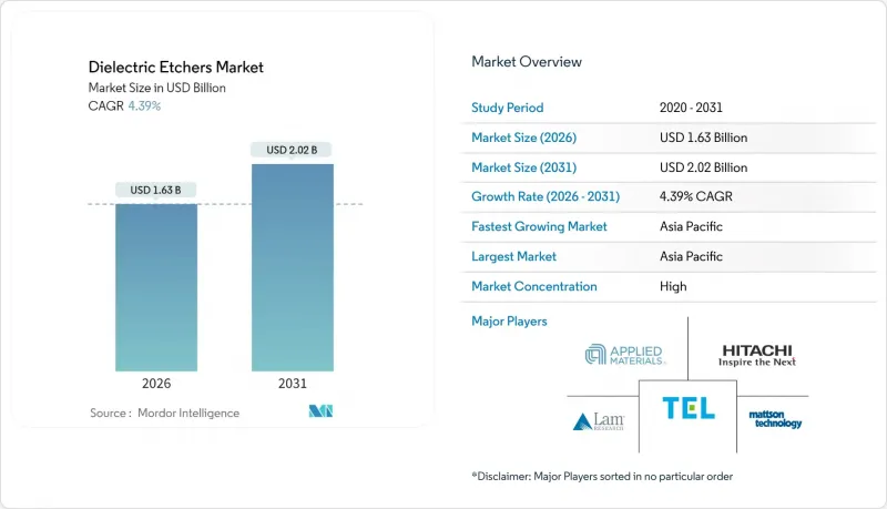
預計到 2026 年,介電蝕刻機市場規模將達到 16.3 億美元,高於 2025 年的 15.6 億美元,預計到 2031 年將達到 20.2 億美元。
預計從 2026 年到 2031 年,其複合年成長率將達到 4.39%。
儘管裝置需求放緩,但對7奈米以下製程原子級精度的需求不斷成長、3D NAND快閃記憶體層數的增加以及先進封裝中低介電常數材料的應用,都將使資本支出居高不下。隨著環柵(GAA)邏輯和異構整合技術的進步縮短了設備更換週期,晶圓代工廠繼續推動介電層蝕刻機市場的發展。從區域來看,舉措佔了設備安裝量的主導地位,但北美CHIPS法案資助的晶圓廠和歐盟的CHIPS計畫正在重塑採購格局。擁有多材料製程技術和國內供應鏈的供應商最能掌握當前的設備更新換代浪潮,而原子層蝕刻(ALE)和低溫等離子體模組等精度增強技術正在開闢新的差異化途徑。
全球介電蝕刻機市場趨勢與洞察
7奈米以下邏輯節點的普及
7nm及以下製程的量產增加了掩模數量並縮小了製程窗口,導致蝕刻步驟數量比10nm製程增加了40%至60%。 GaAs電晶體需要移除犧牲SiGe層,同時不能損壞高k層,這迫使晶圓廠以支援ALE(原子層蝕刻)的裝置取代傳統的蝕刻腔。台積電2025年的380億至420億美元資本支出將主要用於其2nm中試生產線,以確保高選擇性介質模組的多年訂單。隨著製程節點的轉換與封裝技術的更新換代同步進行,設備更新周期將從五年縮短至三年,為介質蝕刻市場帶來穩定的收入。能夠與客戶共同開發化學製程的設備製造商將享有優先供應商地位,從而加強市場進入門檻。
增加3D NAND的層數
在超過400層的堆疊結構中蝕刻64µm深的通道孔,需要接近100:1的長寬比控制,這對等離子體均勻性和副產物排放提出了更高的要求。東京電子計畫於2025年推出低溫蝕刻技術,可減少翹曲和變形,挑戰Lam Research在記憶體蝕刻領域的統治地位。每增加32層,就需要重新設計蝕刻腔,這使得三星等NAND快閃記憶領導企業的更換週期長達18至24個月。這使得介質蝕刻設備市場能夠受益於記憶體投資,即使在邏輯晶片需求疲軟時期也能緩解收入波動。
蝕刻設備資本密集度高
最先進的介質腔造價在500萬至800萬美元之間,而ALE叢集的安裝成本可能高達1200萬至1500萬美元。董事會層級的核准和長期租賃審查導致安裝延遲6至12個月,尤其對於中小型IDM和特種晶圓廠而言更是如此。供應商正在推出模組化平台來應對這項挑戰,這些平台共用射頻、真空和晶圓處理子系統,將成本分攤到各個製程節點,但預算上限仍然使介質刻蝕機市場近期的成長放緩了70個基點。
細分市場分析
到2025年,二氧化矽仍將佔據介電蝕刻機市場38.10%的佔有率,為成熟的邏輯電路和DRAM製程提供支持,在這些流程中,成本成長速度超過了性能成長速度。低介電常數材料用介電蝕刻機的市場規模預計將以468.12%的複合年成長率快速成長,這反映了人工智慧加速器對低電容基板的需求。
低介電常數材料的應用,需要採用避免碳損耗和銅腐蝕的等離子體化學工藝,這推動了多頻射頻技術的創新,而只有現有供應商才能實現大規模商業化。同時,氮化矽和新興玻璃介質在隔離層和麵板級封裝中扮演著獨特的角色,對刻蝕選擇性提出了前所未有的要求。為了滿足這些多樣化的需求,設備製造商必須整合原位終點計量技術和多重壓力腔室,這推高了轉換成本,並維持了介質蝕刻機市場的收入多樣性。
反應離子蝕刻 (RIE) 仍將是成本敏感領域的領導技術,到 2025 年將佔介電蝕刻機市場的 42.26%。然而,原子層蝕刻 (ALEC) 5.02% 的年成長率證實了其在 GAA 電晶體、3D NAND 和量子電路中的必然性。
製造商正在權衡產能損失和產量比率提升。試驗數據顯示,當採用原子層蝕刻 (ALE) 取代鰭片側壁上的多步驟反應離子蝕刻 (RIE) 時,缺陷密度可降低 35% 至 45%。東京電子的低溫 RIE 混合技術模糊了傳統製程與 ALE 的界限,使晶圓廠能夠在保持製程週期預算的同時,策略性地應用 ALE 技術。這種混合化正在使介質蝕刻機市場碎片化,為中型供應商開闢了空間,使其能夠在微波等離子體和紫外線輔助製程等領域開闢新的市場。
區域分析
到2025年,亞太地區將佔介質蝕刻機市場規模的64.51%,這主要得益於韓國記憶體產業和台灣邏輯產業叢集的強勁成長。光是中國大陸就貢獻了Lam Research 42%的收入,但出口限制帶來的不利影響迫使企業採取雙重採購和在地化設備製造策略。日本、印度和新加坡等國政府正大力投資其後端產業生態系統,擴大了區域設備需求,使其超越了傳統市場。
《北美晶片製造法案》(North American CHIPS Act)將在21個州投資超過330億美元,用於支持建造四座新的巨型晶圓廠,每座晶圓廠都需要500多個介電腔室。國內含量條款將提高在美國擁有組裝線的供應商的佔有率,從而促進全球晶片分配模式擺脫對任何單一地區的依賴。
歐洲正透過《歐盟晶片法案》推進自主採購,而德國和法國則吸引了許多大型記憶體和類比電路公司。儘管歐洲大陸的整體市場佔有率落後於亞洲,但由於自主採購模式推動了對綜合工具套件(而非附加組件)需求的成長,其成長速度正在加快。這些變化共同作用,透過地理多元化的收入來源,在區域政策波動的情況下,穩定了介電蝕刻機市場。
其他福利:
- Excel格式的市場預測(ME)表
- 3個月的分析師支持
目錄
第1章 引言
- 研究假設和市場定義
- 調查範圍
第2章調查方法
第3章執行摘要
第4章 市場情勢
- 市場概覽
- 市場促進因素
- 7奈米以下邏輯節點的普及
- 增加3D NAND的層數
- 先進封裝中低介電常數材料的採用
- 對 5G/AI 晶片的需求不斷成長
- 向原子層蝕刻(ALE)過渡
- 政府資助的晶圓廠在地化(晶片法案、歐盟晶片法案等)
- 市場限制
- 蝕刻設備資本密集度高
- 半導體資本投資的週期性
- 新型材料的製程複雜性
- 嚴格的氟碳化合物環境法規
- 產業價值鏈分析
- 監管環境
- 技術展望
- 波特五力分析
- 新進入者的威脅
- 供應商的議價能力
- 買方的議價能力
- 替代品的威脅
- 產業間競爭
第5章 市場規模與成長預測
- 透過介電材料
- 二氧化矽(SiO2)
- 氮化矽(Si3N4)
- 低介電常數絕緣體
- 高介電常數電介質
- 其他成分
- 透過技術
- 反應離子蝕刻(RIE)
- 感應耦合電漿(ICP)
- 原子層蝕刻(ALE)
- 微波電漿蝕刻
- 其他技術
- 按晶圓尺寸
- 150毫米或更小
- 200 mm
- 300 mm
- 超過450毫米
- 最終用戶
- Pure Play Foundry
- 整合設備製造商(IDM)
- MEMS和感測器製造
- 研發及中試生產線
- 按地區
- 北美洲
- 南美洲
- 歐洲
- 亞太地區
- 中東和非洲
第6章 競爭情勢
- 市場集中度
- 策略趨勢
- 市佔率分析
- 公司簡介
- Applied Materials, Inc.
- Lam Research Corporation
- Tokyo Electron Limited
- Hitachi High-Tech Corporation
- ASM International NV
- NAURA Technology Group Co., Ltd.
- Advanced Micro-Fabrication Equipment Inc. China(AMEC)
- SPTS Technologies Ltd.(KLA Corporation)
- Plasma-Therm LLC
- Oxford Instruments plc(Plasma Technology)
- Samco Inc.
- ULVAC, Inc.
- EBARA Corporation
- Dongshin Microelectronics Co., Ltd.
- Beijing Sevenstar Electronics Co., Ltd.
- Mattson Technology, Inc.
- Veeco Instruments Inc.
- Nordson MARCH(Nordson Corporation)
- Trion Technology, Inc.
- Corial SAS
- Plasma Etch, Inc.
- Diener Electronic GmbH and Co. KG
- PVA TePla AG
- Tokuda Seimitsu(Accretech)
- Shenzhen Ideal Energy Equipment Co., Ltd.
第7章 市場機會與未來展望
The dielectric etchers market size in 2026 is estimated at USD 1.63 billion, growing from 2025 value of USD 1.56 billion with 2031 projections showing USD 2.02 billion, growing at 4.39% CAGR over 2026-2031.
Rising atomic-layer precision needs at sub-7 nm, escalating 3D NAND layer counts and low-k dielectric adoption in advanced packaging keep capital spending elevated even when device demand cools. Foundries continue to drive the dielectric etchers market as gate-all-around (GAA) logic and heterogeneous integration shorten equipment replacement cycles. Regionally, Asia Pacific dominates installations, but CHIPS Act-funded fabs in North America and EU Chips initiatives are reshaping procurement geography. Vendors with multi-material process know-how and domestic supply chains are best positioned to capture the current wave of re-tooling, while precision enhancements such as atomic-layer etching (ALE) and cryogenic plasma modules create new differentiation avenues.
Global Dielectric Etchers Market Trends and Insights
Proliferation of Sub-7 nm Logic Nodes
Sub-7 nm production raises mask counts and shrinks process windows, pushing etch step totals 40-60% higher than 10 nm flows. GAA transistors require sacrificial SiGe removal without scarring high-k layers, forcing fabs to swap legacy chambers for ALE-ready tools. TSMC's USD 38-42 billion 2025 capex focuses on 2 nm pilot lines, locking in multi-year orders for high-selectivity dielectric modules. Because node migrations now coincide with packaging overhauls, tool refreshes happen on a three-year rather than five-year cadence, anchoring steady revenue for the dielectric etchers market. Equipment makers that can co-develop chemistries with customers enjoy preferred-supplier status, reinforcing market entry barriers.
3D NAND Layer-Count Escalation
Etching 64 µm-deep channel holes through above 400-layer stacks demands aspect-ratio control near 100:1, pressuring plasma uniformity and by-product evacuation. Cryogenic etch launched by Tokyo Electron in 2025 mitigates bowing and twisting, answering Lam Research's hold in memory etch. Each 32-layer leap forces chamber redesigns, driving an 18-24 month replacement cycle at Samsung and other NAND leaders. The dielectric etchers market therefore benefits from memory spending even during logic lulls, buffering revenue volatility.
High Capital Intensity of Etch Tools
State-of-the-art dielectric chambers cost USD 5-8 million, and ALE clusters can top USD 12-15 million installed. Board-level approvals and extended leasing reviews delay installs 6-12 months, especially at smaller IDMs and specialty fabs. Vendors respond with modular platforms that share RF, vacuum, and wafer-handling subsystems to spread expenses across process nodes, yet budget ceilings still trim the near-term dielectric etchers market expansion rate by 70 basis points.
Other drivers and restraints analyzed in the detailed report include:
- Low-k Dielectric Adoption in Advanced Packaging
- Rising 5G/AI Chip Volumes
- Semiconductor CAPEX Cyclicality
For complete list of drivers and restraints, kindly check the Table Of Contents.
Segment Analysis
Silicon dioxide retained 38.10% dielectric etchers market share in 2025, anchoring mature logic and DRAM flows where cost trumps performance. The dielectric etchers market size for low-k materials is projected to balloon alongside a 468.12% CAGR, reflecting AI accelerators' need for minimal capacitance substrates.
Low-k adoption compels plasma chemistries that avoid carbon depletion and copper corrosion, spurring multi-frequency RF innovations that established vendors alone can commercialize at scale. Simultaneously, silicon nitride and emerging glass dielectrics hold niche roles for barrier and panel-level packaging, demanding etch selectivity previously unseen. This broadening palette obliges toolmakers to bundle in situ endpoint metrology and multi-pressure chambers, reinforcing switching costs and sustaining revenue diversity across the dielectric etchers market.
Reactive-ion etching commanded 42.26% of the dielectric etchers market in 2025 and remains the workhorse for cost-sensitive layers. However, ALE's 5.02% annual growth underscores its inevitability for GAA, 3D NAND and quantum circuits.
Manufacturers weigh throughput penalties against yield gains; pilot data show defect-density cuts of 35-45% when ALE replaces multi-step RIE on fin sidewalls. Tokyo Electron's cryogenic RIE hybrid blurs boundaries, letting fabs phase-in ALE tactically while protecting cycle-time budgets. Such hybridization keeps the dielectric etchers market fragmented, enabling mid-tier suppliers to carve out niches in microwave plasma or UV-assisted processes.
The Global Dielectric Etchers Market Report is Segmented by Dielectric Material (Silicon Dioxide, Silicon Nitride, and More), Technology (Reactive-Ion Etching, Inductively-Coupled Plasma, and More), Wafer Size (less Than 150mm, 200mm, 300mm, and More), End User (Pure-Play Foundries, Idms, MEMS and Sensor Fabs, and R&D and Pilot Lines), and Geography. The Market Forecasts are Provided in Terms of Value (USD).
Geography Analysis
Asia Pacific accounted for 64.51% of dielectric etchers market size in 2025 on the strength of Korean memory and Taiwanese logic clusters. China alone delivered 42% of Lam Research's revenue, yet export-control headwinds compel dual-sourcing and localized toolmaking. Governments across Japan, India and Singapore fund backend ecosystems, widening regional tool demand beyond legacy hubs.
North America's CHIPS Act disperses over USD 33 billion across 21 states, underwriting four green-field mega-fabs that each require more than 500 dielectric chambers. Domestic sourcing clauses open share for suppliers with U.S. assembly lines, nudging global allocation away from single-region dependence.
Europe pursues sovereignty via the EU Chips Act, with Germany and France courting memory and analog giants. Though the continent's aggregate share trails Asia, growth rates accelerate as sovereign procurement pushes comprehensive tool suites rather than add-ons. These shifts collectively steady the dielectric etchers market by diversifying geographic revenue streams against regional policy shocks.
- Applied Materials, Inc.
- Lam Research Corporation
- Tokyo Electron Limited
- Hitachi High-Tech Corporation
- ASM International N.V.
- NAURA Technology Group Co., Ltd.
- Advanced Micro-Fabrication Equipment Inc. China (AMEC)
- SPTS Technologies Ltd. (KLA Corporation)
- Plasma-Therm LLC
- Oxford Instruments plc (Plasma Technology)
- Samco Inc.
- ULVAC, Inc.
- EBARA Corporation
- Dongshin Microelectronics Co., Ltd.
- Beijing Sevenstar Electronics Co., Ltd.
- Mattson Technology, Inc.
- Veeco Instruments Inc.
- Nordson MARCH (Nordson Corporation)
- Trion Technology, Inc.
- Corial SAS
- Plasma Etch, Inc.
- Diener Electronic GmbH and Co. KG
- PVA TePla AG
- Tokuda Seimitsu (Accretech)
- Shenzhen Ideal Energy Equipment Co., Ltd.
Additional Benefits:
- The market estimate (ME) sheet in Excel format
- 3 months of analyst support
TABLE OF CONTENTS
1 INTRODUCTION
- 1.1 Study Assumptions and Market Definition
- 1.2 Scope of the Study
2 RESEARCH METHODOLOGY
3 EXECUTIVE SUMMARY
4 MARKET LANDSCAPE
- 4.1 Market Overview
- 4.2 Market Drivers
- 4.2.1 Proliferation of sub-7 nm logic nodes
- 4.2.2 3D NAND layer-count escalation
- 4.2.3 Low-k dielectric adoption in advanced packaging
- 4.2.4 Rising 5G/AI chip volumes
- 4.2.5 Transition to atomic-layer etching (ALE)
- 4.2.6 Government-funded fab localization (CHIPS Act, EU Chips, etc.)
- 4.3 Market Restraints
- 4.3.1 High capital intensity of etch tools
- 4.3.2 Semiconductor CAPEX cyclicality
- 4.3.3 Process complexity with novel materials
- 4.3.4 Stringent F-gas environmental regulations
- 4.4 Industry Value Chain Analysis
- 4.5 Regulatory Landscape
- 4.6 Technological Outlook
- 4.7 Porter's Five Forces Analysis
- 4.7.1 Threat of New Entrants
- 4.7.2 Bargaining Power of Suppliers
- 4.7.3 Bargaining Power of Buyers
- 4.7.4 Threat of Substitutes
- 4.7.5 Industry Rivalry
5 MARKET SIZE AND GROWTH FORECASTS (VALUE)
- 5.1 By Dielectric Material
- 5.1.1 Silicon Dioxide (SiO2)
- 5.1.2 Silicon Nitride (Si3N4)
- 5.1.3 Low-k Dielectrics
- 5.1.4 High-k Dielectrics
- 5.1.5 Other Materials
- 5.2 By Technology
- 5.2.1 Reactive-Ion Etching (RIE)
- 5.2.2 Inductively-Coupled Plasma (ICP)
- 5.2.3 Atomic-Layer Etching (ALE)
- 5.2.4 Microwave Plasma Etching
- 5.2.5 Other Technologies
- 5.3 By Wafer Size
- 5.3.1 less than or equal to 150 mm
- 5.3.2 200 mm
- 5.3.3 300 mm
- 5.3.4 above 450 mm
- 5.4 By End User
- 5.4.1 Pure-play Foundries
- 5.4.2 Integrated Device Manufacturers (IDMs)
- 5.4.3 MEMS and Sensor Fabs
- 5.4.4 R&D and Pilot Lines
- 5.5 By Geography
- 5.5.1 North America
- 5.5.2 South America
- 5.5.3 Europe
- 5.5.4 Asia Pacific
- 5.5.5 Middle East and Africa
6 COMPETITIVE LANDSCAPE
- 6.1 Market Concentration
- 6.2 Strategic Moves
- 6.3 Market Share Analysis
- 6.4 Company Profiles {(includes Global level Overview, Market level overview, Core Segments, Financials as available, Strategic Information, Market Rank/Share for key companies, Products and Services, and Recent Developments)}
- 6.4.1 Applied Materials, Inc.
- 6.4.2 Lam Research Corporation
- 6.4.3 Tokyo Electron Limited
- 6.4.4 Hitachi High-Tech Corporation
- 6.4.5 ASM International N.V.
- 6.4.6 NAURA Technology Group Co., Ltd.
- 6.4.7 Advanced Micro-Fabrication Equipment Inc. China (AMEC)
- 6.4.8 SPTS Technologies Ltd. (KLA Corporation)
- 6.4.9 Plasma-Therm LLC
- 6.4.10 Oxford Instruments plc (Plasma Technology)
- 6.4.11 Samco Inc.
- 6.4.12 ULVAC, Inc.
- 6.4.13 EBARA Corporation
- 6.4.14 Dongshin Microelectronics Co., Ltd.
- 6.4.15 Beijing Sevenstar Electronics Co., Ltd.
- 6.4.16 Mattson Technology, Inc.
- 6.4.17 Veeco Instruments Inc.
- 6.4.18 Nordson MARCH (Nordson Corporation)
- 6.4.19 Trion Technology, Inc.
- 6.4.20 Corial SAS
- 6.4.21 Plasma Etch, Inc.
- 6.4.22 Diener Electronic GmbH and Co. KG
- 6.4.23 PVA TePla AG
- 6.4.24 Tokuda Seimitsu (Accretech)
- 6.4.25 Shenzhen Ideal Energy Equipment Co., Ltd.
7 MARKET OPPORTUNITIES AND FUTURE OUTLOOK
- 7.1 White-space and Unmet-Need Assessment
 全球蝕刻用矽元件市場(依技術類型、應用、晶圓直徑、終端用戶產業及銷售管道)預測(2026-2032年)矽環和矽電極蝕刻市場:依產品類型、材料類型、應用、最終用途產業和銷售管道分類,全球預測,2026-2032年矽蝕刻組件市場(依產品類型、晶圓直徑、摻雜類型、晶體取向和應用分類),全球預測,2026-2032年
 氫基半導體蝕刻市場分析及預測(至2035年):依類型、產品類型、服務、技術、組件、應用、材料類型、製程、最終用戶、設備分類
 半導體蝕刻設備:市場佔有率分析、產業趨勢與統計、成長預測(2026-2031)
 2026年全球蝕刻機市場報告2026年全球半導體蝕刻設備市場報告
 2026-2030年全球半導體介質蝕刻設備市場全自動電解拋光蝕刻機市場(按組件、類型、應用、最終用戶和分銷管道分類),全球預測(2026-2032年)半導體製造設備矽元件市場(按產品類型、材料類型、設備類型、應用、最終用戶和銷售管道)——2026-2032年全球預測