


 |
市場調查報告書
商品編碼
1631588
亞太地區晶片貼裝設備:市場佔有率分析、產業趨勢、成長預測(2025-2030)APAC Die Attach Equipment - Market Share Analysis, Industry Trends & Statistics, Growth Forecasts (2025 - 2030) |
||||||
價格
※ 本網頁內容可能與最新版本有所差異。詳細情況請與我們聯繫。
簡介目錄
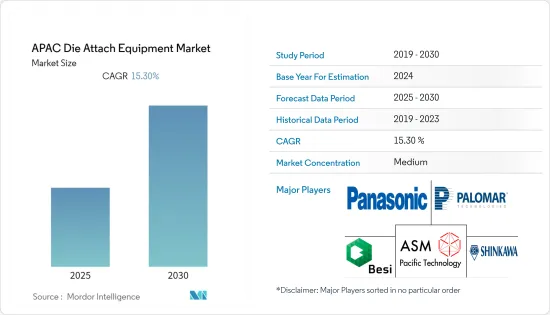
亞太晶片貼裝設備市場預計在預測期內複合年成長率為 15.3%
主要亮點
- 市場供應商下一輪投資的重點將是為小型且高度複雜的 5G 智慧型手機開發晶粒鍵合和封裝解決方案。 5G 是面向未來創新的統一連接平台,可實現持續安全的雲端存取以及顯著更快的資料和視訊傳輸。
- 用戶對 5G 功能的採用將擴大行動寬頻活動,並加速人工智慧在萬物互聯的應用。同樣,用於行動網際網路、計算、5G 和汽車最終用戶的基板和晶圓層次電子構裝製程引領了半導體產業記憶體和邏輯資本支出的復甦。
- 該公司已共用在中長期內增加資本投資,以擴大半導體和 FPD 應用。另一方面,在半導體組裝設備方面,FOWLP/PLP、μLED等高速高精度接合設備的積極開發受到關注。
- BESI共用了針對新數位社會的新組裝技術的投資計劃,包括 FOWLP、TCB、TSV、超薄晶粒、混合鍵合、大面積、晶圓級成型、太陽能和 3D 鋰離子電池電鍍。我們的晶片貼裝設備系列包括單晶片、多晶片、多模組、覆晶、TCB、FOWLP、混合晶粒鍵合系統和晶片分類系統。
- 然而,令人擔憂的是,由於 COVID-19 全球傳播的影響,未來仍存在不確定性。由於 COVID-19 爆發,整個亞太地區的營運關閉和生產暫停對半導體生產和消費產生了重大影響。由於大多數 IDS 和代工廠都位於該地區,因此停產的影響導致資本設備支出減少。這可能會對市場研究產生影響,預計復甦將放緩至 2021 年。
亞太晶片貼裝設備市場趨勢
CIS預計將大幅成長
- CMOS 影像感測器為智慧型手機和其他產品提供了相機功能,但隨著對更小尺寸的需求增加,晶圓廠出現了製造問題。
- 從3G到4G,再到現在的5G,資料效能變得寬頻化,對更高品質相機的需求也不斷增加。由於需要更高的像素數和解析度,這一趨勢推動了 CMOS 影像感測器的堆疊技術的發展。除了這些趨勢之外,生物辨識 ID、3D 感測和增強型人類視覺應用領域也正在促進該領域的成長。
- 客戶對更大更好相機的需求正在推動晶粒尺寸更大的感測器的興起。除了像素縮放之外,CMOS 影像感測器正在經歷晶粒堆疊等技術創新。該市場的供應商使用各種互連技術,例如矽穿孔電極(TSV)、混合鍵合和像素到像素鍵合。
- 例如,在混合鍵合中,晶粒透過銅對銅互連進行連接。為此,在晶圓廠中加工兩片晶圓。一種是邏輯晶圓,另一種是像素陣列晶圓。使用電介質對電介質鍵結然後使用金屬對金屬鍵合將兩個晶片連接起來。
- Xperi 專有的混合結 DBI 技術大量用於三星行動電話的 CMOS 影像感測器的生產。這項用於 CMOS 影像感測器的技術有助於在室溫下實現 Cu-Cu 永久鍵結、低溫退火(~300°C)以及無外部壓力的鍵結製程(電介質/金屬)。
- 在此之前,直接鍵合技術在實現由 Xperifor主導的多代變體的像素縮放(背照式)BSI 和堆疊 BSI 方面發揮了可行的作用超過 15 年。
LED主導市場佔有率
- 晶片黏接材料對於中、高和高功率LED 的性能和可靠性起著至關重要的作用。隨著 LED 滲透率的提高,對晶片貼裝設備的需求不斷增加。針對特定晶片結構和應用選擇適當的晶片貼裝材料取決於多種考慮因素,包括封裝製程(吞吐量和產量比率)、性能(熱輸出和光輸出)、可靠性(流明維持率)和成本。共晶金錫、銀填充環氧樹脂、焊料、矽膠和燒結材料已用於 LED 晶片貼裝。
- SFE提供環氧膠黏合方法,可提供0.2秒/週期的LED環氧固晶機索引時間(90%操作率),晶片尺寸250*250標準,並透過兩個相機識別導線架。其軟體功能包括自動安裝水平儀和拾取水平儀教學功能。
- 此外,導電黏合劑(主要是銀填充環氧樹脂)構成了 LED 熱晶片黏合材料的最大類別(按數量計算)。它們與現有的後端封裝設備相容,並提供有吸引力的成本/性能平衡(通常高達 50W/mK 熱量,具有二次回流焊接相容性)。由於它附著在裸矽上,因此它是無後端金屬化晶片(例如矽基氮化鎵)的最優選材料。
- 此外,儘管LED市場競爭者眾多,ASM是該市場的主要參與企業之一,其LED環氧樹脂高速固晶機AD830在LED市場中佔據主導地位。快速、可靠且準確,晶粒貼裝精度為 +/-1 mil、+/-3 度,小型晶片(如 10 mil x 10 mil)的週期時間為 180 ms,相當於 18,000 UPH。它配備了鍵合後檢查系統,可在預先定義的放置範圍內監控鍵合單元。
亞太地區晶片貼裝設備產業概況
亞太晶片貼裝設備市場競爭適中,眾多公司佔較小的市場佔有率。公司不斷創新並結成策略夥伴關係以維持市場佔有率。
- 2022 年 4 月 - 電氣革命工業化中心 (DER-IC) 東北部接受來自領先的工具和材料技術分銷商 Inseto 的設備,以增強其電力電子、機器和驅動器 (PEMD) 能力。英國安裝的第一台微沖床是 AMX P100 燒結機,它是所提供設備的一部分,能夠生產高度可靠、高功率的模組。
- 2022年6月-West Bond開發了新的7KF鍵合機系列。這家知名公司為微電子封裝產業設計和製造一系列焊線機、晶粒裝機、引線拉伸試驗機、剪切試驗機、超音波元件和配件。這款卓越的工具專為處理射頻、微波、半導體、混合動力和醫療設備領域的困難黏合應用而設計。
其他好處
- Excel 格式的市場預測 (ME) 表
- 3 個月分析師支持
目錄
第1章簡介
- 研究假設和市場定義
- 調查範圍
第2章調查方法
第3章執行摘要
第4章市場動態
- 市場概況
- 產業吸引力-波特五力分析
- 供應商的議價能力
- 買方議價能力
- 新進入者的威脅
- 替代品的威脅
- 競爭公司之間的敵對關係
- 產業價值鏈分析
- COVID-19 對市場的影響
第5章 市場促進因素
- 對 AuSn 共晶晶片貼裝技術的需求不斷成長
- 對分立功率元件的需求
第6章 市場問題
- 加工和壽命期間的尺寸變化和機械不平衡
第7章 市場區隔
- 接合技術
- 固晶機
- 環氧樹脂/黏合劑(糊劑/薄膜)
- 共晶
- 焊接
- 燒結
- 覆晶鍵合機
- 取貨/回流焊接焊接
- 熱壓縮 (TCB)
- 熱超音波黏合
- 混合鍵合
- 固晶機
- 目的
- 記憶
- LED
- 邏輯
- CMOS影像感測器
- 光電子/光電
- 分離式功率元件
- 微機電系統和感測器
- 堆疊記憶體和射頻
- 國家名稱
- 台灣
- 中國
- 日本
- 韓國
- 東南亞
第8章 競爭格局
- 公司簡介
- Palomar Technologies, Inc.
- Shinkawa Ltd
- Panasonic Corporation
- ASM Pacific Technology Limited
- Be Semiconductor Industries NV(Besi)
- Shibaura Mechatronics Corporation
- ficonTEC Trading Ltd(ficonTEC Service GmbH)
- Fasford Technology Co Ltd.
- Dongguan Hoson Electronic Technology Ltd
- For Technos Co., Ltd.
- Shenzhen Xinyichang Technology Co., Ltd.(Hoson)
第 9 章 供應商市場佔有率分析 ~ 2021
第10章投資分析
第11章投資分析市場的未來
簡介目錄
Product Code: 71756
The APAC Die Attach Equipment Market is expected to register a CAGR of 15.3% during the forecast period.
Key Highlights
- A significant focus for the next investment round by market vendors is developing die bonding and packaging solutions for smaller and highly complex 5G compatible smartphones. 5G is a unifying connectivity platform for future innovation, enabling continuous secure cloud access at significantly higher data and video transmission speeds.
- User adoption of 5G capabilities expands mobile broadband activities and accelerates artificial intelligence usage for the Internet of Everything. Likewise, the substrate and wafer-level packaging processes for mobile internet, computing, 5G, and automotive end-user applications drove the semiconductor industry to see a recovery in capital investment for memories and logic.
- The company has shared plans for a medium-to-long-term increase in capital investment towards expanded semiconductor and FPD applications. Whereas, as per Shibaura, active development of high-speed, high-precision bonding equipment for FOWLP / PLP and μLED is being looked out for in semiconductor assembly equipment.
- BESI has shared plans to invest in new assembly technologies such as FOWLP, TCB, TSV, ultra-thin dies, hybrid bonding, large area, wafer level molding, solar, and 3D-lithium-ion battery plating for the new digital society. Its lineup under Die attach equipment includes a single chip, multi-chip, multi-module, flip chip, TCB, FOWLP, hybrid die bonding systems, and die sorting systems.
- However, one source of concern is the continuing uncertain outlook due to the impact of the global spread of COVID-19. Lockdowns and production halts across Asia-pacific due to the COVID-19 outbreak had significantly impacted the production and consumption of semiconductors. With the majority of the IDS and foundries located in the region, the impact of shutdowns has led to reduced spending on capital investments. This is likely to impact the market studied, with a slowed recovery expected across 2021.
APAC Die Attach Equipment Market Trends
CIS is expected to witness significant growth
- CMOS image sensors have been offering camera functions in smartphones and other products, and as the scaling demand grows, the related manufacturing issues in the fab arise.
- The higher-bandwidth data performance progressed from 3G to 4G, and currently, to 5G, the demand for higher quality cameras has grown. This trend has propelled the CMOS image sensor stacking techniques based on the need for higher pixel counts and better resolution. Beyond these trends, the areas of biometric ID, 3D sensing, and enhanced human vision applications have augmented segment growth.
- Customer demand for bigger and better cameras results in more sensors with bigger die sizes. Besides pixel scaling, CMOS image sensors are undergoing other innovations like die stacking. Vendors in the market studied are also using different interconnect technologies, such as through-silicon vias (TSVs), hybrid bonding, and pixel-to-pixel for the same.
- In hybrid bonding, for instance, the dies are connected using copper-to-copper interconnects. For this, two wafers are processed in a fab. One is the logic wafer, while the other is the pixel array wafer. The two wafers are joined using a dielectric-to-dielectric bond, followed by a metal-to-metal connection.
- Hybrid bonding DBI technologies, Xperi'sproprietary technology, are being significantly used by Samsung towards CMOS image sensor fabrication for its phones. This technology for CMOS Image Sensors facilitates room temperature Cu-Cu permanent bonding, low-temperature annealing (around 300°C) & no external pressure bonding process (dielectric/metal).
- Prior to this, direct bond technology has thus played an enabling role in the realization of pixel scaling (backside illumination) BSI and stacked BSI with multiple generational variations led by Xperifor over 15 years.
LED to dominate market share
- Die attach material represents a key role in the performance and reliability of mid, high, and super-high power LEDs. The demand for die-attach equipment is increasing with an increasing LED penetration rate. The selection of suitable die-attach material for a particular chip structure and application depends on various considerations, which include the packaging process (throughput and yield), performance (thermal dissipation output and light output), reliability (lumen maintenance), and cost. Eutectic gold-tin, silver-filled epoxies, solder, silicones, and sintered materials have all been used for LED die attach.
- SFE provides an Epoxy Adhesive bonding method where its LED Epoxy Die Bonder machine features an index time of 0.2 Sec /Cycle (90 Percent Rate of Operation) with a chip size of 250 * 250 standards, providing lead frame recognition through 2 Cameras. Its software function provides auto mount level & pick up level teaching functions.
- Further, conductive adhesives (mostly silver-filled epoxies) constitute the largest class of thermal die-attach materials (by unit number) for LEDs. They are compatible with existing back-end packaging equipment and provide an attractive cost/performance balance (typically up to 50 W/mK thermals with secondary reflow compatibility). As they stick to bare silicon, they are the most preferred material for dies without back-end metallization like GaN on silicon.
- Further, in the LED market, there are a lot of rival competitors, and ASM is one of the prominent players in this market; its LED Epoxy High speed die bonder AD830 dominates in the LED market. It is fast, reliable, and accurate with die placement accuracy of +/-1 mil and +/-3 degree, cycle time for a small chip like 10mil x 10mil is 180 ms, which is an equivalent UPH of 18,000. It is equipped with a Post bond inspection system that monitors the bonded unit at the pre-set placement range.
APAC Die Attach Equipment Industry Overview
The APAC Die attach equipment market is moderately competitive, with a large number of players having a small market share. The companies keep innovating and entering into strategic partnerships to maintain their market share.
- April 2022 - Driving the Electric Revolution Industrialization Centre (DER-IC) North East has received equipment from Inseto, a top technical distributor of tools and materials, to improve its power electronics, machines, and drives (PEMD) capabilities. The first micro-punch machine to be installed in the UK is an AMX P100 sinter press, which is part of the equipment provided and will allow the production of high-reliability, high-power modules.
- June 2022 - The new 7KF Bonder Series has been developed by West Bond. This well-known company designs and manufactures a line of wire bonding and die-to-attach machines, wire pull and shear test equipment, ultrasonic components, and accessories for the microelectronics packaging industry. This excellent tool is made to handle the difficult bonding applications found in the RF, microwave, semiconductor, hybrid, and medical device fields.
Additional Benefits:
- The market estimate (ME) sheet in Excel format
- 3 months of analyst support
TABLE OF CONTENTS
1 INTRODUCTION
- 1.1 Study Assumptions and Market Definition
- 1.2 Scope of the Study
2 RESEARCH METHODOLOGY
3 EXECUTIVE SUMMARY
4 MARKET DYNAMICS
- 4.1 Market Overview
- 4.2 Industry Attractiveness - Porter's Five Forces Analysis
- 4.2.1 Bargaining Power of Suppliers
- 4.2.2 Bargaining Power of Buyers
- 4.2.3 Threat of New Entrants
- 4.2.4 Threat of Substitutes
- 4.2.5 Intensity of Competitive Rivalry
- 4.3 Industry Value Chain Analysis
- 4.4 Impact of Covid-19 on the market
5 Market Drivers
- 5.1 Growing Demand of AuSn Eutectic Die-Attach Technology
- 5.2 Demand of Discrete Power Devices
6 Market Challenges
- 6.1 Dimensional Changes During Processing and Service Life and Mechanical Unbalance
7 MARKET SEGMENTATION
- 7.1 By Bonding Technique
- 7.1.1 Die Bonder
- 7.1.1.1 Epoxy/Adhesive (paste/film)
- 7.1.1.2 Eutectic
- 7.1.1.3 Solder
- 7.1.1.4 Sintering
- 7.1.2 Flip Chip Bonder
- 7.1.2.1 Pick and Place / reflow soldering
- 7.1.2.2 Thermocompresion (TCB)
- 7.1.2.3 Thermosonic Bonding
- 7.1.2.4 Hybrid Bonding
- 7.1.1 Die Bonder
- 7.2 Application
- 7.2.1 Memory
- 7.2.2 LED
- 7.2.3 Logic
- 7.2.4 CMOS Image Sensor
- 7.2.5 Optoelectronics / Photonics
- 7.2.6 Discrete Power Devices
- 7.2.7 MEMS & Sensors
- 7.2.8 Stacked Memory & RF
- 7.3 Country
- 7.3.1 Taiwan
- 7.3.2 China
- 7.3.3 Japan
- 7.3.4 Korea
- 7.3.5 Southeast Asia
8 COMPETITIVE LANDSCAPE
- 8.1 Company Profiles
- 8.1.1 Palomar Technologies, Inc.
- 8.1.2 Shinkawa Ltd
- 8.1.3 Panasonic Corporation
- 8.1.4 ASM Pacific Technology Limited
- 8.1.5 Be Semiconductor Industries NV (Besi)
- 8.1.6 Shibaura Mechatronics Corporation
- 8.1.7 ficonTEC Trading Ltd (ficonTEC Service GmbH)
- 8.1.8 Fasford Technology Co Ltd.
- 8.1.9 Dongguan Hoson Electronic Technology Ltd
- 8.1.10 For Technos Co., Ltd.
- 8.1.11 Shenzhen Xinyichang Technology Co., Ltd. (Hoson)
9 VENDOR MARKET SHARE ANALYSIS - 2021
10 INVESTMENT ANALYSIS
11 FUTURE OF THE MARKET
02-2729-4219
+886-2-2729-4219

