


 |
市場調查報告書
商品編碼
1644604
北美半導體蝕刻設備:市場佔有率分析、行業趨勢和成長預測(2025-2030 年)North America Semiconductor Etch Equipment - Market Share Analysis, Industry Trends & Statistics, Growth Forecasts (2025 - 2030) |
||||||
價格
※ 本網頁內容可能與最新版本有所差異。詳細情況請與我們聯繫。
簡介目錄
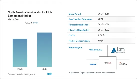
預測期內,北美半導體蝕刻設備市場預計複合年成長率為 4.04%
關鍵亮點
- 北美半導體蝕刻設備市場的成長依賴於半導體晶圓沉積和晶圓加工產業的擴張。由於晶片設計成本上升、新材料、晶片線寬縮小以及製造製程整合的需要,記憶體製造商和代工廠正在加大對更新、更具創新性的設備的投資。例如,2022年2月,德州儀器透露,計畫在2030年在美國半導體晶片生產上投資數十億美元。德州儀器宣布,計畫到 2025 年每年向美國半導體晶片製造業投資 35 億美元。
- 2021 年 3 月,英特爾宣布將在亞利桑那州再建兩座製造工廠(晶圓廠)。在這一消息傳出的背景下,人們擔心全球晶片短缺正在困擾從汽車到電子等各個行業,並且美國在半導體製造業方面落後。該代工廠準備生產一系列採用 ARM 技術的晶片,該技術用於行動設備,歷史上曾與英特爾青睞的 x86 技術競爭。
- 感測器在工業自動化和汽車領域的使用增加了半導體的應用,從而增加了幾乎每個工業領域的需求。這間接提振了半導體蝕刻設備市場。例如,北愛荷華大學(UNI)、揚斯敦州立大學(YSU)和國家國防製造與製造中心(NCDMM)已建立新的合作關係,旨在籌集 1000 萬美元的第一年融資。預計每年有數百家公司將從夥伴關係中受益,透過消除採用積層製造、人工智慧(AI)和機器人等工業 4.0 技術的障礙,在擴大和加強供應鏈的同時增加高品質零件的產量。
- 隨著智慧型手機應用和其他消費品的日益普及,半導體蝕刻設備市場產業正在不斷成長。為了獲得競爭優勢,公司正在加大對製程設備的投資。例如,英特爾將在俄亥俄州投資超過200億美元建造兩家新的晶片工廠。這項投資將大幅提升美國半導體的生產能力,而半導體是電腦、智慧型手機、汽車和其他電子設備的關鍵零件。隨著半導體市場的擴大,半導體蝕刻設備市場也隨之擴大。
- 半導體蝕刻設備產業需要大量的資金,政府的支持在該產業的發展中發揮了至關重要的作用。雖然基於市場的政府支持可以促進創新和技術傳播,但不透明和歧視性的補貼可能會抑制競爭並造成市場扭曲。由於擔心政府針對半導體蝕刻設備製造商的計畫有偏見,製造商不願投資開發優質產品,這限制了市場的發展。
- COVID-19 正在擾亂半導體產業的供應鏈和生產,從而對市場產生負面影響。由於勞動力短缺,半導體蝕刻設備製造商受到的影響更加嚴重。疫情期間,全球半導體供應鏈中的多家公司被迫限制或停止營運。該行業一直在努力應對高虧損和不斷成長的需求,導致供應鏈出現嚴重缺口。
北美半導體蝕刻設備市場趨勢
北美市場正受到美國為避免與中國的貿易摩擦而生產半導體及其相關產品的策略的推動。
- 國內半導體製造對美國政府的運作至關重要。預計新政府將解決日益嚴重的晶片短缺問題,並消除立法者對外包晶片製造使美國更容易受到供應鏈中斷影響的擔憂。拜登啟動了為期100天的審查,新措施和政府支持可能會為美國晶片公司帶來重大提振。因此,北美半導體蝕刻設備市場持續成長。
- 美國晶片需求主要來自大型個人電腦、資訊和通訊基礎設施(包括資料中心和網路設備)、應用市場、智慧型手機和工業設備。蘋果等美國智慧型手機製造商是台積電的主要客戶。美國政府正在尋求500億美元資金支持國內晶片製造。台積電正考慮美國亞利桑那州晶片工廠投入比之前披露金額多數百億美元的資金。此外,台積電預計將與英特爾和三星電子競爭美國政府的建廠補貼。所有這些都為該地區半導體蝕刻設備市場的成長創造了有利的環境。
- 新的美國貿易協定是另一個明顯有利於北美半導體企業的措施。美國的國家技術和工業基礎可以擴大到包括參與企業。此外,美國與歐盟之間的貿易協定,例如《全面與進步協定》(原為TPP)和《跨大西洋貿易和投資夥伴關係》,將降低外國對美國半導體和高科技設備的壁壘,同時增加美國獲得進口半導體相關商品和服務的機會。因此,該地區的半導體蝕刻設備市場預計將擴大。
- 透過美國投資局,美國政府正在與國會兩院合作,提供 520 億美元來刺激私人對半導體市場的投資,並美國美國領先地位。例如SK集團在美國投資新的研發中心、美光公司在美國擴大生產等。預計這將導致該地區半導體蝕刻設備市場的成長。
先進半導體晶片在5G和工業4.0的應用將推動市場成長
- 北美的公司正專注於在工業自動化領域應用5G技術。例如,芝加哥數位製造研究所和國家製造業網路安全中心安裝了私人 5G 網路來連接感測器,以實現工廠設備的自動化、監控和預測性維護。
- 加拿大作為一個商業開放的國家在國際上享有盛譽。加拿大準備採取重要措施,成為未來半導體代工領域的突出地區。此外,該國市場夥伴關係活動也十分活躍。例如,加拿大政府已啟動一項耗資 1.5 億加元的半導體挑戰賽,並向加拿大國家研究委員會投入 9,000 萬加元,用於建立用於通訊網路的光電製造中心。
- 半導體在通訊網路基礎設施中有著應用。為了鼓勵國內生產半導體和半導體蝕刻設備,加拿大政府正在限制外國通訊網路基礎設施供應商在該國的運作。例如,政府已禁止華為和中興的產品和服務在加拿大通訊系統中使用。
- 三星電子計劃在德克薩斯州泰勒市建立一座價值 170 億美元的晶片製造廠。新工廠將生產用於移動、5G、高效能運算和人工智慧的先進製程技術的產品,推動該地區半導體蝕刻設備市場的發展。
- Lam Research Corporation是一家美國晶圓製造設備供應商,致力於開發結合5G和Wi-Fi 6/6E的無線連接。如果這兩種技術處於相同或相近的頻段,那麼建立平行網路將變得極為困難。該公司目前正在提高其氮化鋁薄膜中的鈧摻雜水平(通常在 20% 以上),以提高裝置性能。這顯示該地區半導體蝕刻設備市場技術發展迅速。
北美半導體蝕刻設備產業概況
北美半導體蝕刻設備市場競爭激烈,少數幾家主要企業控制相當一部分市場佔有率。由於所需資本龐大,新進入者很難進入該市場,主要參與者正在透過併購來擴大其市場主導地位。
- 2021 年 9 月,應用材料公司宣布了一項新解決方案,幫助全球領先的碳化矽 (SiC) 晶片製造商從 150 毫米晶圓生產轉向 200 毫米晶圓生產,使每個晶圓的晶粒產量幾乎加倍。
- 2022 年 2 月,泛林集團宣布推出全新選擇性蝕刻產品系列,該產品系列採用突破性的晶圓製造技術和新化學工藝,支援晶片製造商開發環柵 (GAA) 電晶體結構。 Argos(R)、Prevos(TM) 和 Selis(R) 蝕刻產品組合中的三種產品在先進邏輯和記憶體半導體解決方案的設計和製造方面具有顯著的優勢。
- 2022年2月,松下公司採用獨特的捲對捲加工方式,將全球首款兼具低電阻與高透過率的雙面全佈線透明導電膜商業化。採用Panasonic獨特的捲對卷工藝,可以實現傳統蝕刻方法無法實現的2m佈線寬度。
其他福利
- Excel 格式的市場預測 (ME) 表
- 3 個月的分析師支持
目錄
第 1 章 簡介
- 調查結果
- 調查前提
- 研究範圍
第2章調查方法
第3章執行摘要
第4章 市場動態
- 市場概況
- 市場促進因素
- 美國為避免與中國的貿易緊張而採取的國內生產半導體及相關產品的策略
- 先進半導體晶片在5G和工業4.0的應用
- 市場限制
- 缺乏透明度,可能出現歧視性政府補貼
- 價值鏈/供應鏈分析
- 波特五力分析
- 新進入者的威脅
- 購買者/消費者的議價能力
- 供應商的議價能力
- 替代品的威脅
- 競爭對手之間的競爭強度
- COVID-19 對市場的影響
第5章 市場區隔
- 依產品類型
- 高密度蝕刻設備
- 低密度蝕刻設備
- 依蝕刻類型
- 導體蝕刻
- 介電蝕刻
- 多晶矽蝕刻
- 按應用
- 邏輯和記憶
- 功率元件
- MEMS
- 其他
- 按國家
- 美國
- 加拿大
第6章 競爭格局
- 公司簡介
- Applied Materials, Inc
- Hitachi High Technologies America, Inc
- Lam Research Corporation
- SEMES
- Axcelis Technologies, Inc.
- ASM America
- Lattice Semiconductor Corporation
- Texas Instruments
- Panasonic Corporation
第7章投資分析
第 8 章:市場的未來
簡介目錄
Product Code: 90874
The North America Semiconductor Etch Equipment Market is expected to register a CAGR of 4.04% during the forecast period.
Key Highlights
- The growth of the semiconductor Etch Equipment market in North America is dependent on the expansion of the semiconductor wafer deposition and wafer processing sectors. Memory makers and foundries are increasingly focusing on investing in newer and creative equipment due to rising chip design costs, new materials, smaller linewidths on a chip, and the necessity for integrated manufacturing processes. For instance, in February 2022, Texas Instruments detailed its plan to invest billions in U.S. semiconductor chip production through 2030. Texas Instruments revealed plans to invest USD 3.5 billion annually in its U.S. semiconductor chip manufacturing through 2025 as manufacturers face a global shortage of the tech necessary for an increasing number of goods.
- In March 2021, Intel committed to two more new fabrication plants, or fabs, in Arizona. The news comes during a global chip shortage that is snarling industries from automobiles to electronics and worries the United States is falling behind in semiconductor manufacturing. The foundry is poised to manufacture a range of chips based on ARM technology used in mobile devices and has historically competed with Intel's favored x86 technology.
- Industrial automation and the usage of sensors in automotive are increasing the applications of semiconductors and their demand in almost all the industry verticals. Because of this, the Semiconductor Etch Equipment market is rising indirectly. For instance, The University of Northern Iowa (UNI), Youngstown State University (YSU), and the National Center for Defense Manufacturing and Machining (NCDMM) have formed new cooperation that aims to leverage $10 million in first-year financing. Hundreds of businesses are expected to benefit from the partnership each year by removing barriers to adopting Industry 4.0 technologies, such as additive manufacturing, artificial intelligence (AI), and robotics, to increase the output of high-quality parts while expanding and strengthening the supply chain.
- The semiconductor Etch Equipment market industry is growing as smartphone applications and other consumer items become more popular. To achieve a competitive advantage, firms increase their investment in process equipment. For example, Intel will invest more than USD 20 billion in two new chip plants in Ohio. This investment will significantly increase semiconductor manufacturing capabilities in the United States, a critical component of computers, smartphones, automobiles, and other electronic devices. With the increase of the semiconductor market, the semiconductor Etch Equipment market will also increase.
- The semiconductor Etch Equipment industry requires a large amount of cash, and government support has played an essential role in its development. While market-based government support may promote innovation and technological diffusion, non-transparent and discriminatory subsidies can stifle competition and generate market distortions. Fears about skewed government schemes for semiconductor etch equipment makers are constraining market expansion since manufacturers are unwilling to invest in developing high-quality products.
- COVID-19 has negatively impacted the market by disrupting the semiconductor industry's supply chain and production. Due to workforce shortages, the impact on semiconductor etches equipment makers were more severe. Several players in the semiconductor supply chain worldwide had to limit or even cease their operations during the pandemic. The sector was plagued by a high deficit and rising demand, resulting in a considerable supply chain gap.
North America Semiconductor Etch Equipment Market Trends
The United States' strategies for manufacturing semiconductors and peripheral products to avoid trade tensions with China are driving the market in North America.
- Domestic semiconductor manufacturing is essential for the administration of the U.S. government. The new administration is expected to fix the rising chip shortages and address lawmakers' concerns that outsourcing chipmaking had made the United States more vulnerable to supply chain disruptions. In an executive action, Biden started a 100-day review that could significantly boost American chip companies with additional new policies and government support. This is increasing the North American semiconductor Etch Equipment market to grow.
- Most demand for chips in the United States includes large P.C.s and information and communications infrastructure (including data centers and network equipment), application markets, smartphones, and industrial equipment. Smartphone manufacturers based out of the United States, such as Apple, are prominent customers of TSMC. The United States government has called for USD 50 billion in funding to support domestic chip manufacturing. TSMC is weighing plans to pump tens of billions of dollars more into the chip factories in the U.S. state of Arizona than it had previously disclosed. In addition, TSMC is expected to compete against Intel Corp and Samsung Electronics Co Ltd for subsidies from the U.S. government in building the plants. These all create a conducive environment for the growth of the semiconductor Etch Equipment market in the region.
- New U.S. trade agreements are another clear step that would benefit the semiconductor business in North America. The United States National Technology and Industrial Base might be expanded to include allies such as Japan, South Korea, Germany, and the Netherlands, dominant players in the semiconductor supply chain. In addition, trade agreements between the United States and the European Union, such as the Comprehensive and Progressive Trans Partnership (formerly the TPP) and the Transatlantic Trade and Investment Partnership, would increase access to imported semiconductor-related goods and services while lowering foreign barriers to U.S. semiconductors and high-tech devices. Because of this, the semiconductor Etch Equipment market in the region will increase.
- The U.S. Innovation and Competition Act (USICA) and the Administration are working with the House and Senate to provide $52 billion to catalyze more private-sector investments in the semiconductor market and continued American technological leadership. For example, S.K. Group investments in a new R&D center in USA and Micron to expand U.S. production. Due to this, the semiconductor Etch Equipment market in the region will increase.
The application of advanced semiconductor chips in 5G and Industry 4.0 is fostering the market growth
- Companies in the North American region are focusing on implementing 5G technology in Industrial Automations. For example, The Digital Manufacturing Institute and the National Center for Cybersecurity in Manufacturing in Chicago have installed a private 5G network with connections to sensors to automate, monitor, and provide predictive maintenance for factory equipment, which will serve as a real-world model for companies investigating the potential benefits of Industry 4.0 technologies and applications.
- Canada has a significant reputation internationally as a country open for business. It is poised to take essential steps to emerge as a prominent region in the future semiconductor foundry landscape. In addition, the country is witnessing significant partnership activities in the market. For instance, the Canadian government has launched a Canadian Dollar 150 million semiconductor challenge and a Canadian Dollar 90 million to the national research council of Canada for photonics fabrication centers used in the telecommunication network.
- There are applications of semiconductors in communication network infrastructure. To encourage the in-house manufacturing of semiconductors and Semiconductor Etch Equipment, the Canadian government has restricted foreign telecommunication network infra providers from operating in the country. For example, the government prohibits Huawei and ZTE goods and services from being used in Canada's telecommunications systems.
- Samsung Electronics plans to set up a USD 17 billion chip fabrication plant in Taylor, Texas. This new facility will produce goods based on sophisticated process technologies for use in mobile, 5G, high-performance computing, and artificial intelligence, which will drive the Semiconductor Etch Equipment market in the region.
- Lam Research Corporation is an American supplier of wafer fabrication equipment and is working on developing wireless connectivity by combining 5G and Wi-Fi 6/6E. These two technologies in the same or nearby frequency bands will make parallel network setup extremely difficult. Higher scandium doping levels (usually >20 percent) in aluminum nitride films are currently being used by the company to improve device performance. This shows the rampant technological development of the region's semiconductor Etch equipment market.
North America Semiconductor Etch Equipment Industry Overview
The North America Semiconductor Etch Equipment Market is competitive, and few key players contribute to the significant market share. For new entrants, it is difficult to enter this market due to the significant capital required, and significant businesses are pursuing mergers and acquisitions to expand their market dominance.
- In September 2021, Applied Materials, Inc. announced new solutions to help the world's leading silicon carbide (Sic) chipmakers shift from 150mm to 200mm wafer production, which nearly doubles die output per wafer, to help meet the world's growing demand for premium electric vehicle powertrains.
- In Feb 2022, Lam Research Corp announced a new suite of selective etch products that apply breakthrough wafer fabrication techniques and novel chemistries to support chipmakers in developing gate-all-around (GAA) transistor structures. The company's three products, such as Argos(R), Prevos(TM), and Selis(R) etch portfolio, provide a powerful advantage in designing and manufacturing advanced logic and memory semiconductor solutions.
- In Feb 2022, Panasonic Corporation commercialized a double-sided full wiring transparent conductive film combining low resistance and high transmissivity, using its unique roll-to-roll construction method for the first time. Panasonic's original roll-to-roll fabrication approach allowed for a wiring width of 2 m, which was impossible to achieve with traditional etching procedures.
Additional Benefits:
- The market estimate (ME) sheet in Excel format
- 3 months of analyst support
TABLE OF CONTENTS
1 INTRODUCTION
- 1.1 Study Deliverables
- 1.2 Study Assumptions
- 1.3 Scope of the Study
2 RESEARCH METHODOLOGY
3 EXECUTIVE SUMMARY
4 MARKET DYNAMICS
- 4.1 Market Overview
- 4.2 Market Drivers
- 4.2.1 The United States' strategies for the manufacturing in-house semiconductors and peripheral products to avoid trade tensions with China
- 4.2.2 The application of advanced semiconductor chips in 5G and Industry 4.0
- 4.3 Market Restraints
- 4.3.1 Non-transparent and chance of Government discriminatory subsidies
- 4.4 Value Chain / Supply Chain Analysis
- 4.5 Porter's Five Forces Analysis
- 4.5.1 Threat of New Entrants
- 4.5.2 Bargaining Power of Buyers/Consumers
- 4.5.3 Bargaining Power of Suppliers
- 4.5.4 Threat of Substitute Products
- 4.5.5 Intensity of Competitive Rivalry
- 4.6 COVID-19 Impact on the Market
5 MARKET SEGMENTATION
- 5.1 By Product Type
- 5.1.1 High-density Etch Equipment
- 5.1.2 Low-density Etch Equipment
- 5.2 By Etching Type
- 5.2.1 Conductor Etching
- 5.2.2 Dielectric Etching
- 5.2.3 Polysilicon Etching
- 5.3 By Application
- 5.3.1 Logic and Memory
- 5.3.2 Power Devices
- 5.3.3 MEMS
- 5.3.4 Others
- 5.4 Country
- 5.4.1 United States
- 5.4.2 Canada
6 COMPETITIVE LANDSCAPE
- 6.1 Company Profiles
- 6.1.1 Applied Materials, Inc
- 6.1.2 Hitachi High Technologies America, Inc
- 6.1.3 Lam Research Corporation
- 6.1.4 SEMES
- 6.1.5 Axcelis Technologies, Inc.
- 6.1.6 ASM America
- 6.1.7 Lattice Semiconductor Corporation
- 6.1.8 Texas Instruments
- 6.1.9 Panasonic Corporation
7 Investment Analysis
8 Future of the Market
02-2729-4219
+886-2-2729-4219
 全球蝕刻用矽元件市場(依技術類型、應用、晶圓直徑、終端用戶產業及銷售管道)預測(2026-2032年)矽環和矽電極蝕刻市場:依產品類型、材料類型、應用、最終用途產業和銷售管道分類,全球預測,2026-2032年矽蝕刻組件市場(依產品類型、晶圓直徑、摻雜類型、晶體取向和應用分類),全球預測,2026-2032年
 氫基半導體蝕刻市場分析及預測(至2035年):依類型、產品類型、服務、技術、組件、應用、材料類型、製程、最終用戶、設備分類
 介質蝕刻機:市場佔有率分析、產業趨勢與統計、成長預測(2026-2031)半導體蝕刻設備:市場佔有率分析、產業趨勢與統計、成長預測(2026-2031)
 2026年全球蝕刻機市場報告2026年全球半導體蝕刻設備市場報告
 2026-2030年全球半導體介質蝕刻設備市場全自動電解拋光蝕刻機市場(按組件、類型、應用、最終用戶和分銷管道分類),全球預測(2026-2032年)
▼