


 |
市場調查報告書
商品編碼
1699355
光刻設備市場機會、成長動力、產業趨勢分析及2025-2034年預測Lithography Equipment Market Opportunity, Growth Drivers, Industry Trend Analysis, and Forecast 2025-2034 |
||||||
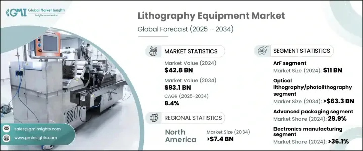
2024 年全球光刻設備市場價值為 428 億美元,預計 2025 年至 2034 年的複合年成長率為 8.4%。這一成長是由對先進和緊湊半導體元件的需求激增所推動的,尤其是在消費性電子產品領域。隨著現代電子設備的不斷發展,製造商正在突破半導體設計的界限,以提高處理能力、能源效率和整體性能。這種日益成長的複雜性推動了尖端光刻技術的採用,確保了具有卓越功能的高密度晶片的生產。
半導體產業的晶片製造流程正在快速進步,光刻設備在下一代設備中發揮著至關重要的作用。人工智慧、物聯網 (IoT) 和 5G 技術的日益融合,進一步擴大了對高效能晶片的需求,對先進的光刻解決方案產生了強勁的需求。此外,半導體產業的競爭性質導致光刻技術不斷創新,使製造商能夠在半導體製造中實現更高的精度和效率。隨著半導體產業朝向更複雜的架構發展,對光刻設備的依賴不斷擴大,使其成為技術進步的關鍵驅動力。
| 市場範圍 | |
|---|---|
| 起始年份 | 2024 |
| 預測年份 | 2025-2034 |
| 起始值 | 428億美元 |
| 預測值 | 931億美元 |
| 複合年成長率 | 8.4% |
市場按技術細分為 ArF、KrF、i-line、ArF 浸沒式和極紫外線 (EUV) 微影。其中,ArF 領域在 2024 年的價值為 110 億美元,並將實現顯著成長,特別是由於其在視訊串流、線上遊戲以及虛擬和擴增實境等快速成長的行業中的應用。 ArF 技術在深紫外線 (DUV) 微影領域提供了增強的性能,這對於生產高性能、高密度半導體裝置至關重要。隨著對強大而高效的晶片的需求不斷增加,ArF 領域預計將進一步擴大,並加強其在推動半導體創新方面的作用。
光刻設備進一步按類型分類,包括光學微影、電子束微影、光罩對準器、離子光刻、X光微影和奈米壓印微影。其中,光學光刻技術(也稱為照相平版印刷技術)仍然佔據主導地位,預計到 2034 年將達到 633 億美元。其廣泛採用歸因於它可以無縫整合到現有的半導體生產設施中,使其成為晶片製造商具有成本效益且可擴展的解決方案。隨著解析度和效率的不斷提高,光學光刻技術仍然是半導體製造的首選,確保了其在未來幾年的強大市場地位。
北美光刻設備市場將大幅成長,預計到 2034 年將達到 74 億美元。這一成長是由汽車、消費性電子和資料中心等產業對半導體的需求不斷成長所推動的。加強供應鏈彈性和將半導體製造帶回國內的努力正在進一步推動市場擴張。此外,北美對研發的重視,加上高技能勞動力,正在加速光刻技術的創新,使該地區成為半導體進步的關鍵樞紐。
目錄
第1章:方法論與範圍
第2章:執行摘要
第3章:行業洞察
- 產業生態系統分析
- 產業衝擊力
- 成長動力
- 消費性電子產品對先進、微型半導體元件的需求不斷成長
- 光刻工藝的技術進步
- 汽車電氣化需求不斷成長,電動車在全球普及
- 全球物聯網和人工智慧技術日益流行
- 對緊湊型和節能設備的需求不斷成長
- 產業陷阱與挑戰
- 生產成本高
- 安全問題
- 成長動力
- 成長潛力分析
- 監管格局
- 技術格局
- 未來市場趨勢
- 差距分析
- 波特的分析
- PESTEL分析
第4章:競爭格局
- 介紹
- 公司市佔率分析
- 主要市場參與者的競爭分析
- 競爭定位矩陣
- 策略儀表板
第5章:市場估計與預測:按技術,2021 年至 2034 年
- 主要趨勢
- 氬氟
- 氪氟
- i線
- Arf 浸入式
- 極紫外線 (EUV) 微影
第6章:市場估計與預測:按設備,2021 年至 2034 年
- 主要趨勢
- 光學光刻/光刻
- 掩模對準器
- 電子束光刻
- 離子光刻
- X光光刻
- 奈米壓印光刻
第7章:市場估計與預測:按應用,2021 年至 2034 年
- 主要趨勢
- 先進封裝
- MEMS 設備
- LED 設備
- 其他
第8章:市場估計與預測:依最終用途,2021 年至 2034 年
- 主要趨勢
- 電子製造業
- 醫療保健和生命科學
- 汽車產業
- 電信
- 其他
第9章:市場估計與預測:按地區,2021 年至 2034 年
- 主要趨勢
- 北美洲
- 美國
- 加拿大
- 歐洲
- 英國
- 德國
- 法國
- 義大利
- 西班牙
- 亞太地區
- 中國
- 日本
- 印度
- 韓國
- 澳新銀行
- 台灣
- 拉丁美洲
- 巴西
- 墨西哥
- 中東和非洲
- 沙烏地阿拉伯
- 阿拉伯聯合大公國
- 以色列
- 南非
第10章:公司簡介
- ASML Holding NV
- Nikon Corporation
- Canon Inc.
- Veeco Instruments Inc.
- SUSS MicroTec AG
- EV Group
- SCREEN Holdings Co., Ltd.
- Onto Innovation Inc.
- JEOL Ltd
- Neutronix Quintel Inc. (NXQ)
- Advantest
- Shanghai Micro Electronics Equipment (Group) Co., Ltd.
The Global Lithography Equipment Market was valued at USD 42.8 billion in 2024 and is projected to grow at a CAGR of 8.4% from 2025 to 2034. This growth is fueled by the surging demand for advanced and compact semiconductor components, particularly in consumer electronics. As modern electronic devices continue to evolve, manufacturers are pushing the boundaries of semiconductor design to enhance processing power, energy efficiency, and overall performance. This growing complexity is driving the adoption of cutting-edge lithography technologies, ensuring the production of high-density chips with superior functionality.
The semiconductor industry is experiencing rapid advancements in chip manufacturing processes, with lithography equipment playing a crucial role in enabling next-generation devices. The increasing integration of artificial intelligence, the Internet of Things (IoT), and 5G technology is further amplifying the need for high-performance chips, creating a strong demand for advanced lithography solutions. Moreover, the competitive nature of the semiconductor industry has led to continuous innovation in lithography techniques, allowing manufacturers to achieve higher precision and efficiency in semiconductor fabrication. As the semiconductor industry moves toward more intricate architectures, the reliance on lithography equipment continues to expand, making it a key driver of technological progress.
| Market Scope | |
|---|---|
| Start Year | 2024 |
| Forecast Year | 2025-2034 |
| Start Value | $42.8 Billion |
| Forecast Value | $93.1 Billion |
| CAGR | 8.4% |
The market is segmented by technology into ArF, KrF, i-line, ArF immersion, and Extreme Ultraviolet (EUV) Lithography. Among these, the ArF segment was valued at USD 11 billion in 2024 and is set for significant growth, particularly due to its applications in fast-growing industries like video streaming, online gaming, and virtual and augmented reality. ArF technology delivers enhanced performance within Deep Ultraviolet (DUV) lithography, which is essential for producing high-performance, high-density semiconductor devices. As the need for powerful and efficient chips increases, the ArF segment is expected to expand further, reinforcing its role in driving semiconductor innovation.
Lithography equipment is further categorized by type, including optical lithography, electron beam lithography, mask aligners, ion lithography, X-ray lithography, and nanoimprint lithography. Among these, optical lithography, also known as photolithography, remains the dominant segment and is projected to reach USD 63.3 billion by 2034. Its widespread adoption is attributed to its seamless integration into existing semiconductor production facilities, making it a cost-effective and scalable solution for chipmakers. With continuous advancements improving resolution and efficiency, optical lithography remains a preferred choice for semiconductor manufacturing, ensuring its strong market presence in the years ahead.
North America lithography equipment market is set for substantial growth, projected to reach USD 7.4 billion by 2034. This surge is driven by rising semiconductor demand across industries such as automotive, consumer electronics, and data centers. Efforts to strengthen supply chain resilience and bring semiconductor manufacturing back to domestic regions are further fueling market expansion. Additionally, North America's emphasis on research and development, coupled with a highly skilled workforce, is accelerating innovation in lithography technology, positioning the region as a key hub for semiconductor advancements.
Table of Contents
Chapter 1 Methodology and Scope
- 1.1 Market scope and definitions
- 1.2 Research design
- 1.2.1 Research approach
- 1.2.2 Data collection methods
- 1.3 Base estimates and calculations
- 1.3.1 Base year calculation
- 1.3.2 Key trends for market estimation
- 1.4 Forecast model
- 1.5 Primary research and validation
- 1.5.1 Primary sources
- 1.5.2 Data mining sources
Chapter 2 Executive Summary
- 2.1 Industry 360° synopsis
Chapter 3 Industry Insights
- 3.1 Industry ecosystem analysis
- 3.2 Industry impact forces
- 3.2.1 Growth drivers
- 3.2.1.1 Rising demand for advanced and miniaturized semiconductor components in consumer electronics
- 3.2.1.2 Technological advancements in the lithography process
- 3.2.1.3 Increasing demand for electrification in vehicles and the global proliferation of electric vehicles
- 3.2.1.4 Increasing trend toward IoT and AI technology around the globe
- 3.2.1.5 Growing demand for Compact and Power-Efficient Devices
- 3.2.2 Industry pitfalls and challenges
- 3.2.2.1 High production cost
- 3.2.2.2 Security concerns
- 3.2.1 Growth drivers
- 3.3 Growth potential analysis
- 3.4 Regulatory landscape
- 3.5 Technology landscape
- 3.6 Future market trends
- 3.7 Gap analysis
- 3.8 Porter's analysis
- 3.9 PESTEL analysis
Chapter 4 Competitive Landscape, 2024
- 4.1 Introduction
- 4.2 Company market share analysis
- 4.3 Competitive analysis of major market players
- 4.4 Competitive positioning matrix
- 4.5 Strategy dashboard
Chapter 5 Market Estimates and Forecast, By Technology, 2021 – 2034 (USD Mn)
- 5.1 Key trends
- 5.2 ArF
- 5.3 KrF
- 5.4 i-line
- 5.5 Arf immersion
- 5.6 Extreme Ultraviolet (EUV) Lithography
Chapter 6 Market Estimates and Forecast, By Equipment, 2021 – 2034 (USD Mn)
- 6.1 Key trends
- 6.2 Optical Lithography/Photolithography
- 6.3 Mask aligners
- 6.4 Electron beam lithography
- 6.5 Ion lithography
- 6.6 X-Ray lithography
- 6.7 Nanoimprint lithography
Chapter 7 Market Estimates and Forecast, By Application, 2021 – 2034 (USD Mn)
- 7.1 Key trends
- 7.2 Advanced packaging
- 7.3 MEMS devices
- 7.4 LED devices
- 7.5 Others
Chapter 8 Market Estimates and Forecast, By End Use, 2021 – 2034 (USD Mn)
- 8.1 Key trends
- 8.2 Electronics manufacturing
- 8.3 Healthcare and Life sciences
- 8.4 Automotive industry
- 8.5 Telecommunications
- 8.6 Others
Chapter 9 Market Estimates and Forecast, By Region, 2021 – 2034 (USD Mn)
- 9.1 Key trends
- 9.2 North America
- 9.2.1 U.S.
- 9.2.2 Canada
- 9.3 Europe
- 9.3.1 UK
- 9.3.2 Germany
- 9.3.3 France
- 9.3.4 Italy
- 9.3.5 Spain
- 9.4 Asia Pacific
- 9.4.1 China
- 9.4.2 Japan
- 9.4.3 India
- 9.4.4 South Korea
- 9.4.5 ANZ
- 9.4.6 Taiwan
- 9.5 Latin America
- 9.5.1 Brazil
- 9.5.2 Mexico
- 9.6 Middle East and Africa
- 9.6.1 Saudi Arabia
- 9.6.2 UAE
- 9.6.3 Israel
- 9.6.4 South Africa
Chapter 10 Company Profiles
- 10.1 ASML Holding N.V.
- 10.2 Nikon Corporation
- 10.3 Canon Inc.
- 10.4 Veeco Instruments Inc.
- 10.5 SUSS MicroTec AG
- 10.6 EV Group
- 10.7 SCREEN Holdings Co., Ltd.
- 10.8 Onto Innovation Inc.
- 10.9 JEOL Ltd
- 10.10 Neutronix Quintel Inc. (NXQ)
- 10.11 Advantest
- 10.12 Shanghai Micro Electronics Equipment (Group) Co., Ltd.
 100奈米以下光刻:全球市場分析與策略課題
 全球 i-Line 步進機市場:趨勢、預測和競爭分析(至 2031 年)
 全球曝光機設備市場:市場規模、佔有率、趨勢分析報告 - 按類型、按應用、按技術、按封裝平台、按地區、展望和預測,2024-2031
 2030 年微影術設備市場預測:按技術、製程類型、組件、波長、應用、最終用戶和地區進行的全球分析
 下一代光刻材料市場:按類型、技術和最終用戶分類 - 2025-2030 年全球預測全球微影術設備市場:按類型、技術、封裝平台、應用和最終用戶 - 預測(2025-2030)
 全球微影術系統市場,2024-2028下一代光刻材料市場,按材料、按應用、按最終用戶、按國家和地區分類 - 2024-2032 年行業分析、市場規模、市場佔有率和預測
 微影材料的全球市場(重要材料),2024~2025年
 新一代光刻材料市場 - 全球產業規模、佔有率、趨勢、機會和預測,按材料、應用、地區和競爭細分,2019-2029F