


 |
市場調查報告書
商品編碼
1479763
100奈米以下光刻:全球市場分析與策略課題Sub-100nm Lithography: Market Analysis and Strategic Issues |
||||||
促進因素
隨著半導體技術節點的縮小以及對更小、更複雜的半導體裝置的需求的增加,多種驅動因素□□正在推動光刻技術的進步,以應對這些課題。
技術擴展:對於每個新技術節點,半導體製造商的目標是縮小電晶體和互連的尺寸,以提高效能、功率效率和密度。 為了實現這種高精度和高解析度的小型化,先進的光刻技術必不可少,並且正在推動下一代光刻工具的開發。
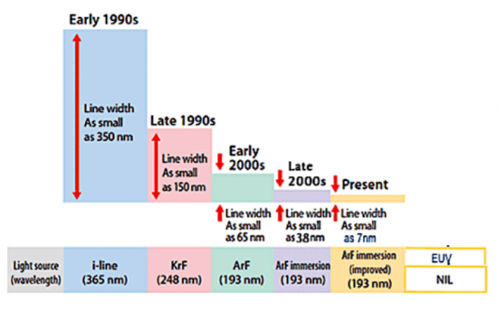
使用EUV微影:EUV微影的波長比傳統光學微影更短,因此可以形成更精細、更複雜的圖案。 隨著節點變得更小,為了實現所需的圖案分辨率,採用 EUV 光刻變得越來越必要。
多重圖案化技術:隨著特徵尺寸接近光學微影的極限,SADP、SAQP 和MBML 等多重圖案化技術對於實現所需的特徵密度和間距變得至關重要。 這些技術需要多次曝光和蝕刻步驟來創建複雜的圖案,增加了對先進光刻解決方案的需求。
解析度增強技術(RET):為了提高圖案轉移的解析度和保真度,光刻工具包括光學鄰近校正(OPC)、相移掩模(PSM)、來源整合瞭解析度增強技術例如掩模優化(SMO)。 這些 RET 有助於減輕衍射和其他光學限制的影響,從而能夠在先進節點中製造更精細的特徵。
提高製程控制和產量:隨著特徵尺寸的減小,保持嚴格的製程控製成為越來越大的課題。 先進的光刻工具結合了先進的計量和製程控制功能,以確保均勻性、覆蓋精度和減少缺陷。 這些功能對於在先進節點實現高產量和製造一致性至關重要。
新興應用和市場需求:人工智慧、5G 連接、自動駕駛汽車和物聯網設備等新興技術正在推動對具有特定性能要求的專用半導體設備的需求。 先進的光刻解決方案對於這些應用所需的複雜結構和材料的圖案化至關重要,並且正在推動光刻技術的創新。
需要此報告
半導體光刻是半導體製造的基石,也是製造支援現代電子產品的複雜半導體裝置的極其重要的製程。 隨著半導體技術的進步,光刻技術也在進步,突破瞭解析度、精準度和產量的極限,使得製造更精細、更複雜的半導體結構成為可能。
由於對更高性能和節能電子設備的需求,半導體產業正在表現出對小型化的不懈追求。 極紫外線 (EUV) 微影、多重圖案化和浸沒式微影等先進微影技術在實現亞 10 奈米尺寸、突破半導體製造能力的極限方面發揮關鍵作用。
本報告對全球半導體光刻市場進行了全面分析,深入瞭解市場規模、成長動力、競爭格局和新的市場機會。
目錄
第一章簡介
第 2 章執行摘要
- 主要問題摘要
- 市場機會摘要
第 3 章光刻技術的問題與趨勢
- 光學系統
- 簡介
- 步進重複對準器
- 深層紫外線 (DUV)
- 極紫外光
- 奈米壓印光刻
- X射線光刻
- 電子束光刻
- 離子束光刻
第 4 章使用者與供應商策略
- 確定您的光刻需求
- 供應商基準
- 價格
- 供應商的承諾與態度
- 供應商能力
- 系統功能
- 設備評估期間供應商的回饋
- 設備生產過程中供應商的回饋
- 競爭環境
- 1級無塵室設備
- 未來工廠的設備
- 機會
第五章市場預測
- 促進因素
- 技術趨勢
- 經濟趨勢
- 光學限制
- 市場預測的假設
- 市場預測
Driving Forces
As semiconductor technology nodes shrink and demand for smaller and more complex semiconductor devices increases, several driving forces push the advancement of lithography technology to meet these challenges:
Technological Scaling: With each new technology node, semiconductor manufacturers aim to reduce the size of transistors and interconnects to improve performance, power efficiency, and density. Advanced lithography techniques are essential for patterning these smaller features with high precision and resolution, driving the development of next-generation lithography tools.
EUV Lithography Adoption: Extreme ultraviolet (EUV) lithography has emerged as a leading candidate for patterning critical layers in advanced semiconductor manufacturing processes. EUV offers shorter wavelengths than traditional optical lithography, enabling the fabrication of smaller feature sizes and more complex patterns. As nodes get smaller, the adoption of EUV lithography becomes increasingly necessary to achieve the required patterning resolution.
Multi-Patterning Techniques: As feature sizes approach the limits of optical lithography, multipatterning techniques such as self-aligned double patterning (SADP), self-aligned quadruple patterning (SAQP), and multi-beam maskless lithography (MBML) become indispensable for achieving the desired feature density and pitch. These techniques involve multiple exposure and etching steps to create intricate patterns, driving the need for advanced lithography solutions.
Resolution Enhancement Technologies (RET): To improve the resolution and fidelity of pattern transfer, lithography tools incorporate resolution enhancement techniques such as optical proximity correction (OPC), phase-shift masks (PSM), and source mask optimization (SMO). These RETs help mitigate the effects of diffraction and other optical limitations, enabling the fabrication of finer features at advanced nodes.
Process Control and Yield Improvement: As feature sizes shrink, maintaining tight process control becomes increasingly challenging. Advanced lithography tools incorporate sophisticated metrology and process control capabilities to ensure uniformity, overlay accuracy, and defect reduction. These capabilities are essential for achieving high yields and manufacturing consistency at advanced nodes.
Emerging Applications and Market Demand: Emerging technologies such as artificial intelligence (AI), 5G connectivity, autonomous vehicles, and IoT devices drive the demand for specialized semiconductor devices with specific performance requirements. Advanced lithography solutions are essential for patterning the complex structures and materials required for these applications, driving innovation in lithography technology.
The Need for This Report
Semiconductor lithography stands as a cornerstone in the realm of semiconductor manufacturing, serving as a pivotal process in the creation of intricate semiconductor devices that power modern electronics. As semiconductor technology advances, lithography techniques evolve in tandem, pushing the boundaries of resolution, precision, and throughput to enable the fabrication of ever-smaller and more complex semiconductor structures. This comprehensive report delves into the multifaceted landscape of semiconductor lithography, exploring key technologies, market trends, industry challenges, and future prospects shaping the semiconductor lithography ecosystem.
The semiconductor industry is witnessing a relentless pursuit of miniaturization, driven by the demand for higher-performance and more energy-efficient electronic devices. As feature sizes shrink to nanoscale dimensions, lithography emerges as a critical enabler, allowing semiconductor manufacturers to pattern intricate circuit designs with unparalleled precision. Advanced lithography techniques such as extreme ultraviolet (EUV) lithography, multiple patterning, and immersion lithography play pivotal roles in achieving sub-10 nanometer feature sizes, pushing the limits of semiconductor manufacturing capabilities.
In addition to technological advancements, the semiconductor lithography market is influenced by a myriad of factors, including market dynamics, regulatory policies, and industry collaborations. This report provides a comprehensive analysis of the global semiconductor lithography market, offering insights into market size, growth drivers, competitive landscape, and emerging opportunities. Through a detailed examination of lithography equipment, materials, and processes, stakeholders gain a deeper understanding of the evolving semiconductor lithography landscape and its impact on the semiconductor industry.
Furthermore, the report explores key challenges and bottlenecks facing semiconductor lithography, ranging from mask complexity and defect reduction to cost constraints and yield optimization. By identifying critical issues and potential solutions, stakeholders can devise strategies to mitigate risks and capitalize on growth opportunities in the semiconductor lithography market.
As semiconductor lithography continues to evolve in response to technological advancements and market demands, stakeholders across the semiconductor ecosystem must stay abreast of the latest developments and trends shaping the industry. This report serves as a valuable resource for semiconductor manufacturers, equipment suppliers, investors, and other industry participants seeking actionable insights into the dynamic landscape of semiconductor lithography. Through comprehensive analysis and strategic recommendations, this report empowers stakeholders to navigate the complex terrain of semiconductor lithography and drive innovation in semiconductor manufacturing.
Report Coverage
This report provides a detailed analysis of the global semiconductor lithography market, including historical data, current market size, and projected growth trends. It may also include market segmentation based on technology, end-user industry, and geographical regions.
It explores the various lithography technologies utilized in semiconductor manufacturing, such as optical lithography, extreme ultraviolet (EUV) lithography, multiple patterning, nanoimprint lithography, and others. This section delves into the principles, advancements, and applications of each technology.
Market Segmentation: Unit and Revenue segments the semiconductor lithography market based on technology types are forecast by:
|
|
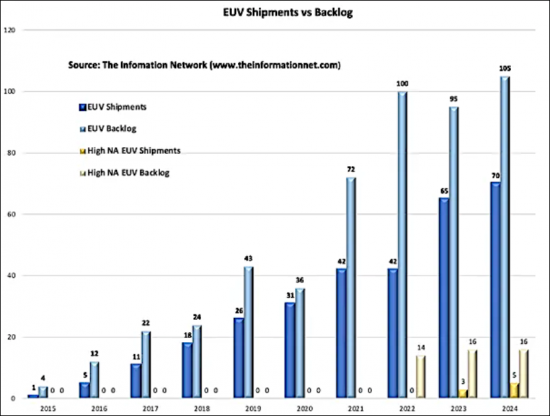
The report provides insights into market share of lithography vendors by equipment type including revenue and unit shipments. Market shares by vendor are provided since 1992. The report identifies and analyzes current and emerging trends driving the semiconductor lithography market, such as node migration, China sanctions, and new semiconductor materials, particularly silicon carbide.
Table of Contents
Chapter 1. Introduction
- 1.1. The Need For This Report
Chapter 2. Executive Summary
- 2.1. Summary of Major Issues
- 2.2. Summary of Market Opportunities
Chapter 3. Lithography Issues And Trends
- 3.1. Optical Systems
- 3.1.1. Introduction
- 3.1.2. Step-and-Repeat Aligners
- 3.1.3. Deep Ultraviolet (DUV)
- 3.2. EUV
- 3.5. Nano-Imprint Lithography
- 3.4. X-Ray Lithography
- 3.3. Electron Beam Lithography
- 3.4. Ion Beam Lithography
Chapter 4. User - Supplier Strategies
- 4.1. Determining Lithography Needs
- 4.2. Benchmarking a Vendor
- 4.2.1. Pricing
- 4.2.2. Vendor Commitment and Attitudes
- 4.2.3. Vendor Capabilities
- 4.2.4. System Capabilities
- 4.2.5. Vendor Feedback During Equipment Evaluation
- 4.2.6. Vendor Feedback During Device Production
- 4.3. Competitive Environment
- 4.4. Equipment For Class 1 Cleanrooms
- 4.5. Equipment For the Factory of the Future
- 4.6. Opportunities
Chapter 5. Market Forecast
- 5.1. Driving Forces
- 5.1.1. Technical Trends
- 5.1.2. Economic Trends
- 5.1.3. Optical Limitations
- 5.2. Market Forecast Assumptions
- 5.3. Market Forecast
List of Tables
- 3.1. Wavelength "Generations"
- 3.2. Characteristics of X-Ray Systems
- 5.1. Worldwide Capital Spending
- 5.2. DRAM Lithographic Requirements
- 5.3. Worldwide Optical Stepper Market
- 5.4. Worldwide Stepper Market Shares
List of Figures
- 1.1. Lithographic Equipment Requirements for DRAMs
- 3.1. Lithography Options For MPUs/DRAMs
- 3.2. Lithography Options For Flash
- 3.3. Illustration of Stepper Exposure System
- 3.4. Lens Arrangement For Submicron Features
- 3.5. Excimer Laser Evolution
- 3.6. EUV Lithography
- 3.7. Thermoplastic Nanoimprint Lithography Process
- 3.8. Step And Flash Nanoimprint Lithography Process
- 3.9. Illustration of X-Ray Lithography
- 3.10. Schematic Of Scalpel Electron Beam System
- 3.11. Multi-Source E-Beam Lithography
- 3.12. Ion Projection Lithography System
- 4.1. Manufacturing Costs Per Exposure Station
- 5.1. Lithography Market Vs Equipment Market
- 5.2. Lithography Double Exposure Technique
- 5.3. Lithography Requirements
- 5.4. Lithography Extensions
- 5.5. Lithography Cost of Ownership
- 5.6. Segmentation of Stepper/Scan Shipments
- 5.7. Market Shares of Vendors (Units)
- 5.8. Unit Market Shares of Vendors
- 5.9. Worldwide I-Line Market Shares
- 5.10. Worldwide 248nm Market Shares
- 5.11. Worldwide 193nm Dry Market Shares
- 5.12. Worldwide 193nm Wet Market Shares
- 5.13. Market Shares of Vendors (Revenues)
 光刻設備市場機會、成長動力、產業趨勢分析及2025-2034年預測
 全球 i-Line 步進機市場:趨勢、預測和競爭分析(至 2031 年)
 全球曝光機設備市場:市場規模、佔有率、趨勢分析報告 - 按類型、按應用、按技術、按封裝平台、按地區、展望和預測,2024-2031
 2030 年微影術設備市場預測:按技術、製程類型、組件、波長、應用、最終用戶和地區進行的全球分析
 下一代光刻材料市場:按類型、技術和最終用戶分類 - 2025-2030 年全球預測全球微影術設備市場:按類型、技術、封裝平台、應用和最終用戶 - 預測(2025-2030)
 全球微影術系統市場,2024-2028下一代光刻材料市場,按材料、按應用、按最終用戶、按國家和地區分類 - 2024-2032 年行業分析、市場規模、市場佔有率和預測
 微影材料的全球市場(重要材料),2024~2025年
 新一代光刻材料市場 - 全球產業規模、佔有率、趨勢、機會和預測,按材料、應用、地區和競爭細分,2019-2029F