


 |
市場調查報告書
商品編碼
1473282
應用材料公司:目標市場競爭分析Applied Materials: Competitive Analysis of Served Markets |
||||||
介紹
應用材料公司憑藉其技術領先地位、戰略市場定位以及應對現代半導體製造課題的全面方法,在競爭激烈的半導體製造設備行業中脫穎而出。隨著半導體產業朝向更小的節點和更複雜的裝置架構發展,應用材料公司在蝕刻、沉積、CMP、計量和離子注入設備方面的創新將在實現下一代電子裝置方面發揮重要作用。透過持續創新和策略遠見,應用材料公司正在引領半導體技術和製造的未來,使我們在每個市場都擁有無與倫比的領導地位。
蝕刻/沉積技術
應用材料公司在作為半導體裝置製造基礎的蝕刻和沈積過程方面表現出色。該公司的蝕刻設備精確控制等離子體工藝,這對於在矽基板上定義奈米級特徵至關重要。
在氣相沉積方面,我們提供化學氣相沉積 (CVD)、物理氣相沉積 (PVD) 和原子層沉積 (ALD) 解決方案。這些技術對於形成半導體裝置的各種薄膜層至關重要,並且重點關注精度、製程效率以及對不斷變化的行業要求的適應性。
化學機械研磨設備
CMP(化學機械拋光)設備也是應用材料公司重點關注的領域,可確保製造步驟之間的晶圓表面平整度。應用材料公司的 CMP 設備整合到製造工作流程中,以優化產量並降低廢品率。這有助於提高製造產量和成本效率,並實現半導體產業的目標。
測量/檢測設備
計量和檢測設備提供有關晶圓特性的關鍵數據,促進製程調整和缺陷的早期檢測。此類設備對於品質控制至關重要,使製造商能夠在設備變得更加複雜的情況下保持高產品產量和營運效率。
離子注入機
應用材料公司也專注於離子注入技術,這對於摻雜半導體材料至關重要。
該公司的注入機對於精確控制摻雜劑種類、能量和劑量以實現半導體裝置所需的電氣性能至關重要。
關於本報告
本報告分析了應用材料公司在全球半導體製造設備市場的表現趨勢,包括整體技術開發、製造和供應趨勢(2012-2023)、依產品類型劃分的市場規模和佔有率以及主要競爭對手。產品和業務成果。
目錄
第一章簡介
第二章 應用材料戰略
- 市場策略
- 推動製造設備需求
- 國際存在
- 滿足客戶需求
- 新任CEO的策略
- 經營策略
- Silicon Systems Group
- Applied Global Services
- 展示
- 能源和環境解決方案
- 技術戰略
- 產品策略
- 收購策略
- 法律策略
- 財務分析
第三章市場預測
- 市場驅動力
- 半導體市場
- 技術趨勢
- 經濟趨勢
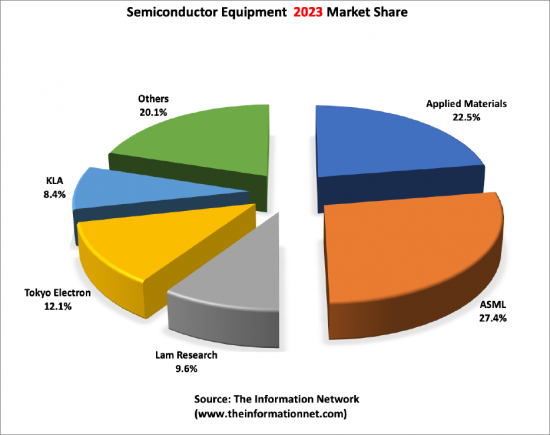
- Applied Materials:全球市場領導者(截至 2019 年)
- 市場規模及市佔率
- 化學氣相沉積
- 物理氣相沉積
- 乾蝕刻
- 快速熱處理/氧化/擴散
- 矽外延
- CMP(化學機械平坦化)
- 測量/檢查
- 離子注入
第四章競爭環境
- 介紹
- Lam Research
- Tokyo Electron Limited
- KLA
- ASM International
- Axcelis
- Canon Anelva
- Ebara
- Eugene Technology
- Hitachi High-Technologies
- Hitachi Kokusai Electric
- Jusung Engineering
- KC Tech
- Lasertec
- Nissin Ion Equipment
- NuFlare Technology
- Screen Semiconductor Solutions
- SEMES
- SEN
- TES
- Ulvac
- Wonik IPS
Introduction
In the competitive realm of semiconductor manufacturing equipment, Applied Materials stands out for its technological leadership, strategic market positioning, and comprehensive approach to addressing the challenges of modern semiconductor fabrication. As the industry moves towards smaller nodes and more complex device architectures, Applied Materials' innovations in etch, deposition, CMP, metrology, and ion implant equipment will continue to play a critical role in enabling the next generation of electronic devices. Through continuous innovation and strategic foresight, Applied Materials is not just competing but leading in the markets it serves, shaping the future of semiconductor technology and manufacturing.
Applied Materials' market leadership is supported by continuous innovation and a strategic approach to addressing semiconductor manufacturing challenges. The company's investment in research and development ensures its technologies meet current demands and anticipate future industry shifts.
As semiconductor fabrication evolves towards more advanced nodes and explores novel materials and architectures, Applied Materials is poised to play a central role. Its comprehensive technology portfolio, covering etch, deposition, CMP, metrology/inspection, and ion implant, positions the company as a key enabler of next-generation semiconductor devices.
Etch and Deposition Technologies
Applied Materials excels in etch and deposition processes, foundational to semiconductor device fabrication. The company's etch systems offer precise control over plasma processes, crucial for defining nanoscale features on silicon substrates. These systems enable the creation of intricate device structures required for current computing and memory applications.
In deposition, Applied Materials provides solutions across Chemical Vapor Deposition (CVD), Physical Vapor Deposition (PVD), and Atomic Layer Deposition (ALD). These technologies are critical for forming the various thin-film layers in semiconductor devices, with a focus on precision, process efficiency, and adaptability to evolving industry requirements.
CMP Systems
CMP equipment is another area of focus for Applied Materials, ensuring the planarity of wafer surfaces between fabrication steps. The company's CMP systems integrate with fabrication workflows, optimizing throughput and reducing defectivity. This contributes to improved manufacturing yields and cost efficiencies, aligning with the semiconductor industry's goals.
Metrology/Inspection Equipment
Metrology and inspection equipment from Applied Materials provides critical data on wafer properties, facilitating process adjustments and early defect identification. This category of equipment is vital for quality control, enabling manufacturers to uphold high standards of product yield and operational efficiency amid increasing device complexity.Ion Implant Equipment
Applied Materials also specializes in ion implantation technology, essential for doping semiconductor materials. The company's implanters deliver high precision in dopant species, energy, and dose control, critical for achieving desired electrical characteristics in semiconductor devices.
About This Report
This report addressed the Served Available Markets that Applied Materials competes. Namely:
- Chemical Vapor Deposition
- Physical Vapor Deposition
- Dry Etch
- Rapid Thermal Processing/Oxidation/Diffusion
- Silicon Epitaxy
- Chemical Mechanical Planarization
- Metrology and Inspection
- Ion Implantation
It presents forecasts for each sector and market shares for each equipment type between 2012 and 2023.
Table of Contents
Chapter 1. Introduction
Chapter 2. Applied's Strategies
- 2.1. Market Strategies
- 2.1.1. Driving Demand for Processing Equipment
- 2.1.2. A Global Presence
- 2.1.3. Meeting Customer Needs
- 2.1.4. New CEO's Strategy
- 2.2. Business Strategies 2.
- 2.2.1. Silicon Systems Group
- 2.2.2. Applied Global Services
- 2.2.3. Display
- 2.2.4. Energy and Environmental Solutions
- 2.3. Technology Strategies
- 2.4. Product Strategies
- 2.5. Acquisition Strategies
- 2.6. Legal Strategies
- 2.7. Financial Analysis
Chapter 3. Market Forecast
- 3.1. Market Drivers
- 3.1.1. Semiconductor Market
- 3.1.2. Technical Trends
- 3.1.3. Economic Trends
- 3.2. Applied Materials - Global Market Leader Until 2019
- 3.3. Market Size and Market Shares
- 3.3.1. Chemical Vapor Deposition
- 3.3.2. Physical Vapor Deposition
- 3.3.3. Dry Etch
- 3.3.4. Rapid Thermal Processing/Oxidation/Diffusion
- 3.3.5. Silicon Epitaxy
- 3.3.6. Chemical Mechanical Planarization
- 3.3.7. Metrology and Inspection
- 3.3.8. Ion Implantation
Chapter 4. Competitive Environment
- 4.1. Introduction
- 4.2. Lam Research
- 4.2.1. Strategies
- 4.2.2. Products
- 4.2.3. Financial Analysis
- 4.3. Tokyo Electron Limited
- 4.3.1. Strategies
- 4.3.2. Products
- 4.3.3. Financial Analysis
- 4.4. KLA
- 4.4.1. Strategies
- 4.4.2. Products
- 4.4.3. Financial Analysis
- 4.5. ASM International
- 4.5.1. Strategies
- 4.5.2. Products
- 4.5.3. Financial Analysis
- 4.6. Axcelis
- 4.6.1. Strategies
- 4.6.2. Products
- 4.6.3. Financial Analysis
- 4.7. Canon Anelva
- 4.7.1. Business Sectors Covered In The Market Analysis Chapter
- 4.7.2. Company Profile
- 4.7.3. Company Financials
- 4.8. Ebara
- 4.8.1. Business Sectors Covered In The Market Analysis Chapter
- 4.8.2. Company Profile
- 4.8.3. Company Financials
- 4.9. Eugene Technology
- 4.9.1. Business Sectors Covered In The Market Analysis Chapter
- 4.9.2. Company Profile
- 4.9.3. Company Financials
- 4.10. Hitachi High-Technologies
- 4.10.1. Business Sectors Covered In The Market Analysis Chapter
- 4.10.2. Company Profile
- 4.10.3. Company Financials
- 4.11. Hitachi Kokusai Electric
- 4.11.1. Business Sectors Covered In The Market Analysis Chapter
- 4.11.2. Company Profile
- 4.11.3. Company Financials
- 4.12. Jusung Engineering
- 4.12.1. Business Sectors Covered In The Market Analysis Chapter
- 4.12.2. Company Profile
- 4.12.3. Company Financials
- 4.13. KC Tech
- 4.13.1. Business Sectors Covered In The Market Analysis Chapter
- 4.13.2. Company Profile
- 4.13.3. Company Financials
- 4.14. Lasertec
- 4.14.1. Business Sectors Covered In The Market Analysis Chapter
- 4.14.2. Company Profile
- 4.14.3. Company Financials
- 4.15. Nissin Ion Equipment
- 4.15.1. Business Sectors Covered In The Market Analysis Chapter
- 4.15.2. Company Profile
- 4.15.3. Company Financials
- 4.16. NuFlare Technology
- 4.16.1. Business Sectors Covered In The Market Analysis Chapter
- 4.16.2. Company Profile
- 4.16.3. Company Financials
- 4.17. Screen Semiconductor Solutions
- 4.17.1. Business Sectors Covered In The Market Analysis Chapter
- 4.17.2. Company Profile
- 4.17.3. Company Financials
- 4.18. SEMES
- 4.18.1. Business Sectors Covered In The Market Analysis Chapter
- 4.18.2. Company Profile
- 4.18.3. Company Financials
- 4.19. SEN
- 4.19.1. Business Sectors Covered In The Market Analysis Chapter
- 4.19.2. Company Profile
- 4.19.3. Company Financials
- 4.20. TES
- 4.20.1. Business Sectors Covered In The Market Analysis Chapter
- 4.20.2. Company Profile
- 4.20.3. Company Financials
- 4.21. Ulvac
- 4.21.1. Business Sectors Covered In The Market Analysis Chapter
- 4.21.2. Company Profile
- 4.21.3. Company Financials
- 4.22. Wonik IPS
- 4.22.1. Business Sectors Covered In The Market Analysis Chapter
- 4.22.2. Company Profile
- 4.22.3. Company Financials
List of Tables
- 3.1. Worldwide Capital Spending
- 3.2. Wafer Front End (WFE) Market By Device Type
- 3.3. Top Semiconductor Equipment Revenues
- 3.4. Worldwide CVD Market Forecast
- 3.5. Worldwide CVD Market Shares
- 3.6. Worldwide PVD Market Forecast
- 3.7. Worldwide PVD Market Shares
- 3.8. Worldwide Dry Etch Market Forecast
- 3.9. Worldwide Dry Etch Market Shares
- 3.10. Worldwide RTP/Oxidation/Diffusion Market Forecast
- 3.11. Worldwide RTP/Oxidation/Diffusion Market Shares
- 3.12. Worldwide Silicon Epitaxy Market Forecast
- 3.13. Worldwide Silicon Epitaxy Market Shares
- 3.14. Worldwide CMP Market Forecast
- 3.15. Worldwide CMP Market Shares
- 3.16. Worldwide M&I Market Forecast
- 3.17. Worldwide M&I Market Shares
- 3.18. Worldwide Ion Implantation Market Forecast
- 3.19. Worldwide Ion Implantation Market Shares
List of Figures
- 3.1. Semiconductor vs Equipment vs GDP
- 3.2. Recession Cycle
- 3.3. Semiconductor Equipment Share
- 3.4. Worldwide CVD Market Shares
- 3.5. Worldwide PVD Market Shares
- 3.6. Worldwide Dry Etch Market Shares
- 3.7. Worldwide RTP/Oxidation/Diffusion Market Shares
- 3.8. Worldwide Silicon Epitaxy Market Shares
- 3.9. Worldwide CMP Market Shares
- 3.10. Worldwide M&I Market Shares
- 3.11. Worldwide Ion Implantation Market Shares
 半導體資本設備市場-全球產業規模、佔有率、趨勢、機會和預測(按類型、應用、最終用戶、地區和競爭格局分類),2020-2030年預測
 全球半導體製造設備市場:微影術、晶圓表面處理、晶圓清洗、沉積、組裝與封裝、切割、計量、鍵合、晶圓檢測/整合電路檢測、記憶體、邏輯電路、分立元件、類比電路——預測至2032年
 2025年全球二手半導體設備市場報告2025年全球半導體後端設備市場報告2025年全球半導體製造設備前端(FOL)市場報告
 中國大陸半導體及設備市場:分析及製造趨勢
 全球半導體製造設備:市場、市場佔有率、市場預測
 全球半導體製造設備市場(按類型、應用和地區劃分)-市場規模、產業趨勢、機會分析及預測(2025-2033 年)
 IC前端雷射退火設備:全球市佔率及排名、總收入及需求預測(2025-2031年)半導體模具清洗橡膠片:全球市佔率及排名、總收入及需求預測(2025-2031年)