


 |
市場調查報告書
商品編碼
1479761
等離子蝕刻:市場分析與策略問題Plasma Etching: Market Analysis and Strategic Issues |
||||||
半導體等離子體蝕刻是半導體製造的關鍵工藝,受到多種因素的推動,這些因素反映了行業不斷變化的需求、技術進步和市場動態。
隨著對摩爾定律的不斷追求以及對更小、更強大的半導體裝置的需求,不斷需要減小特徵尺寸並增加裝置密度。 等離子蝕刻可以實現奈米級的精確圖案轉移,從而有助於製造高精度和先進的半導體結構。
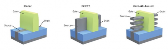
半導體裝置正在演變成日益複雜的架構,例如 FinFET、3D NAND 快閃記憶體和多層互連,並且需要先進的蝕刻技術來實現所需的裝置形狀和功能。 等離子蝕刻提供了對複雜的多層、多維裝置結構進行圖案化所需的靈活性和控制。
隨著半導體材料變得更加多樣化,化合物半導體裝置變得越來越流行,對能夠有效蝕刻各種材料同時保持高選擇性和均勻性的等離子體蝕刻製程的需求不斷增長。 透過開發專門的蝕刻化學物質和製程配方,可以精確控製材料去除率和側壁輪廓,以確保最佳的裝置性能和可靠性。
5G 無線通訊、人工智慧 (AI)、物聯網 (IoT) 和自動駕駛汽車等新應用和技術的激增正在推動對具有特定性能特徵和功能的半導體裝置的需求。 等離子蝕刻可以客製化和優化裝置結構,以滿足這些應用的要求,開闢新的市場機會並促進半導體製造的創新。
半導體產業競爭激烈,製造商爭奪市場佔有率、技術領先地位和創新。 在激烈的市場競爭的推動下,等離子蝕刻設備、材料和製程技術的不斷進步正在突破蝕刻能力和性能的極限,以滿足不斷變化的客戶需求並獲得競爭優勢。
隨著技術的快速進步和市場需求的不斷增加,半導體等離子體蝕刻領域正在經歷前所未有的演變和創新。 設備製造商、材料供應商和半導體公司不斷突破等離子蝕刻技術的極限,以滿足半導體裝置日益增長的複雜性和性能要求。 從提高製程均勻性和生產率到擴大可蝕刻的材料和裝置結構的範圍,半導體等離子體蝕刻產業處於技術創新的前沿,推動著電子產業的進步和塑造未來。
本報告考察了等離子蝕刻市場,深入研究了等離子蝕刻技術的複雜性,並探討了其基本原理、關鍵應用以及塑造產業的新興趨勢。 它還包括對市場動態、技術創新和競爭格局的詳細分析。
目錄
第一章簡介
第 2 章執行摘要
第三章技術問題與趨勢
- 簡介
- 處理問題
- 等離子剝離
- 安全性問題
第四章市場預測
第 5 章策略問題:使用者
- 評估使用者需求
- 供應商基準
- 成本分析
- 使用者與供應商的協同作用
第 6 章策略問題:供應商
- 衝突
- 與客戶互動
- 1 級無塵室的設備相容性
- 佔地面積和可維護性
- 細懸浮微粒的產生
- 自動化
- 蝕刻工具
Driving Forces
Semiconductor plasma etching, a critical process in semiconductor manufacturing, is driven by a multitude of factors that reflect the evolving demands of the industry, technological advancements, and market dynamics. These driving forces encompass various aspects of semiconductor fabrication and the broader semiconductor ecosystem:
Device Scaling and Miniaturization: With the relentless pursuit of Moore's Law and the demand for smaller, more powerful semiconductor devices, there is a continuous need to shrink feature sizes and increase device density. Plasma etching enables precise pattern transfer at nanometer scales, facilitating the fabrication of advanced semiconductor structures with high precision and accuracy.
Complex Device Architectures: The evolution of semiconductor devices towards increasingly complex architectures, such as FinFETs, 3D NAND flash memory, and multi-layer interconnects, necessitates advanced etching techniques to achieve the desired device geometries and functionality. Plasma etching offers the flexibility and control required to pattern intricate device structures with multiple layers and dimensions.
Material Compatibility and Selectivity: As semiconductor materials diversify and compound semiconductor devices gain prominence, there is a growing need for plasma etching processes that can effectively etch a wide range of materials while maintaining high selectivity and uniformity. The development of specialized etching chemistries and process recipes enables precise control over material removal rates and sidewall profiles, ensuring optimal device performance and reliability.
Yield Enhancement and Process Control: Semiconductor manufacturers place a premium on yield enhancement and process control to minimize defects, improve device performance, and optimize production efficiency. Plasma etching plays a critical role in achieving these objectives by enabling precise pattern transfer with minimal variability, thereby reducing defect density, enhancing device uniformity, and maximizing wafer yields.
Emerging Applications and Technologies: The proliferation of emerging applications and technologies, such as 5G wireless communication, artificial intelligence (AI), Internet of Things (IoT), and autonomous vehicles, drives demand for semiconductor devices with specific performance characteristics and functionality. Plasma etching enables the customization and optimization of device structures to meet the requirements of these applications, opening up new market opportunities and driving innovation in semiconductor manufacturing.
Market Competition and Technological Innovation: The semiconductor industry is highly competitive, with manufacturers vying for market share, technological leadership, and innovation. Continuous advancements in plasma etching equipment, materials, and process technologies are driven by intense market competition, pushing the boundaries of etching capabilities and performance to meet evolving customer demands and gain competitive advantage.
Trends
Technological trends in semiconductor plasma etching are continuously evolving to address the growing demands of the semiconductor industry for higher performance, increased functionality, and enhanced manufacturability. Several key trends are driving innovation in plasma etching technologies:
Sub-Nanometer Feature Control: With the ongoing push towards smaller feature sizes and higher device densities, there is a critical need for plasma etching techniques capable of achieving sub-nanometer feature control. Advanced plasma sources, such as inductively coupled plasma (ICP) and electron cyclotron resonance (ECR), enable precise control over ion energy and flux, facilitating the etching of ultrafine features with sub-nanometer accuracy.
Selective Etching and Material Compatibility: As semiconductor devices incorporate a wider range of materials, including compound semiconductors, dielectrics, and metals, there is a growing demand for plasma etching processes that offer high selectivity and compatibility with diverse materials. Selective etching chemistries and process recipes enable the precise removal of target materials while minimizing damage to underlying layers and interfaces, ensuring optimal device performance and reliability.
Anisotropic Etching and Sidewall Control: Anisotropic etching, which produces vertical sidewalls with minimal sidewall roughness, is essential for fabricating advanced semiconductor structures with precise dimensions and profiles. Advanced plasma etching techniques, such as reactive ion etching (RIE) and deep reactive ion etching (DRIE), enable precise sidewall control and profile customization, facilitating the fabrication of complex device architectures, such as FinFETs, nanowires, and 3D memory structures.
Damage-Free Etching and Low-K Dielectric Preservation: With the increasing use of low-k dielectric materials in semiconductor devices to minimize signal delay and crosstalk, there is a growing emphasis on damage-free etching techniques that preserve the integrity of these sensitive materials. Plasma etching processes, such as downstream plasma etching and cryogenic etching, offer reduced ion energy and temperature, minimizing damage to low-k dielectrics and preserving their electrical properties.
Etch-Depth Uniformity and Across-Wafer Variability: Achieving uniform etch depths and minimizing across-wafer variability are critical for ensuring consistent device performance and yield in semiconductor manufacturing. Advanced plasma etching systems incorporate real-time process monitoring and control capabilities, such as optical emission spectroscopy (OES) and endpoint detection, to achieve precise etch-depth uniformity and minimize variations across the wafer, enhancing process repeatability and yield.
High-Aspect-Ratio Etching and Through-Silicon Via (TSV) Fabrication: The increasing demand for high-aspect-ratio structures, such as through-silicon vias (TSVs) and microelectromechanical systems (MEMS), requires plasma etching techniques capable of etching deep, narrow features with high aspect ratios. Deep silicon etching (DSE) and Bosch process-based etching enable the fabrication of TSVs and MEMS devices with precise control over sidewall profiles, aspect ratios, and etch depths, facilitating the integration of 3D device architectures and heterogeneous integration.
The Need for This Report
The semiconductor industry stands at the forefront of technological innovation, driving progress across various sectors from consumer electronics to healthcare and automotive. At the heart of semiconductor manufacturing lies the intricate process of plasma etching, a critical step in device fabrication that defines the intricate features and structures of modern semiconductor devices. As the demand for smaller, faster, and more energy-efficient electronic devices continues to soar, the importance of semiconductor plasma etching in enabling the production of advanced semiconductor devices cannot be overstated.
Plasma etching plays a pivotal role in the fabrication of semiconductor devices by selectively removing material layers from semiconductor substrates with unparalleled precision and control. By harnessing the unique properties of plasma—a highly ionized gas composed of charged particles—semiconductor manufacturers can achieve sub-micron feature sizes and complex device architectures essential for next-generation electronic applications. From logic and memory chips to advanced sensors and power devices, plasma etching technology underpins the development of a wide range of semiconductor products that drive innovation in virtually every aspect of modern life.
Against the backdrop of rapid technological advancements and growing market demands, the semiconductor plasma etching landscape is witnessing unprecedented evolution and innovation. Equipment manufacturers, materials suppliers, and semiconductor companies alike are continually pushing the boundaries of plasma etching technology to address the increasing complexity and performance requirements of semiconductor devices. From enhancing process uniformity and productivity to expanding the range of materials and device structures that can be etched, the semiconductor plasma etching industry is at the forefront of innovation, driving progress and shaping the future of electronics.
In this comprehensive report on semiconductor plasma etching, we delve into the intricacies of plasma etching technology, exploring its fundamental principles, key applications, and emerging trends shaping the industry. Through a detailed analysis of market dynamics, technological innovations, and competitive landscape, this report provides valuable insights and strategic intelligence for stakeholders across the semiconductor ecosystem. Whether you are a semiconductor equipment manufacturer, materials supplier, semiconductor company, or industry analyst, this report serves as a comprehensive guide to understanding the latest developments and opportunities in the dynamic field of semiconductor plasma etching.
About This Report
This 150-page report provides a comprehensive analysis of the semiconductor plasma etching market, including market size, growth drivers, challenges, and opportunities. Assessment of the competitive landscape, key players, market segmentation by product type, application, and geography.
Major segments are forecast with current and historic market shares are:
- Dielectric Etch
- Conductive Etch
- Plasma Strip
This report explores the wide range of applications of plasma etching in semiconductor manufacturing, including etching of silicon, compound semiconductors, dielectrics, metals, and other materials. Specific applications in logic devices, memory devices, sensors, power devices, and other semiconductor products.
Insights into the future outlook for semiconductor plasma etching technology, including emerging applications, market trends, and growth opportunities are detailed.
Table of Contents
Chapter 1. Introduction
- 1.1. The Need For This Report
Chapter 2. Executive Summary
- 2.1. Summary of Technical Issues
- 2.2. Summary of User Issues
- 2.3. Summary of Supplier Issues
- 2.4. Summary of Market Forecasts
Chapter 3. Technical Issues and Trends
- 3.1. Introduction
- 3.2. Processing Issues
- 3.2.1. Chlorine Versus Fluorine Processes
- 3.2.2. Multilevel Structures
- 3.2.3. New Materials
- 3.2.4. GaAs Processing
- 3.3. Plasma Stripping
- 3.3.1. Photoresist Stripping
- 3.3.2. Low-K Removal
- 3.4. Safety Issues
- 3.4.1. System Design Considerations
- 3.4.2. Gas Handling
- 3.4.3. Reactor Cleaning
Chapter 4. Market Forecast
- 4.1. Influence of Technology Trends on the Equipment Market
- 4.2. Market Forecast Assumptions
- 4.3. Market Forecast
Chapter 5. Strategic Issues: Users
- 5.1. Evaluating User Needs
- 5.1.1. Device Architecture
- 5.1.2. Wafer Starts and Throughput Requirements
- 5.1.3. Wafer Size
- 5.2. Benchmarking a Vendor
- 5.2.1. Pricing
- 5.2.2. Vendor Commitment and Attitudes
- 5.2.3. Vendor Capabilities
- 5.2.4. System Capabilities
- 5.3. Cost Analysis
- 5.3.1. Equipment Price
- 5.3.2. Installation Costs
- 5.3.3. Maintenance Costs
- 5.3.4. Sustaining Costs
- 5.3.5. Hidden Costs
- 5.4. User - Supplier Synergy
- 5.4.1. Feedback During Equipment Evaluation
- 5.4.2. Feedback During Device Production
Chapter 6. Strategic Issues: Suppliers
- 6.1. Competition
- 6.2. Customer Interaction
- 6.2.1. Customer Support
- 6.2.2. Cleanroom Needs in the Applications Lab
- 6.3. Equipment Compatibility in Class 1 Cleanrooms
- 6.3.1. Footprint Versus Serviceability
- 6.3.2. Particulate Generation
- 6.3.3. Automation
- 6.3.4. Etch Tools
List of Figures
- 3.1. Various Enhanced Designs (a) Helicon, (b) Multiple ECR, (c) Helical Resonator
- 3.2. Schematic of Inductively Coupled Plasma Source
- 3.3. Schematic of the HRe Source
- 3.4. Schematic of the Dipole Magnet Source
- 3.5. Schematic of Chemical Downstream Etch
- 3.6. Silicon Trench Structure
- 3.7. fin/STI Etch Requirements
- 3.8. FinFET Gate Etch Requirements
- 3.9. Dual Damascene Dielectric Etch Approaches
- 4.1. Trends in Minimum Feature Size for Dynamic RAMS
- 4.2. Market Shares for Dry Etch Equipment
- 4.3. Market Shares for Strip Equipment
- 4.4. Distribution of Etch Sales by Type
- 4.5. Distribution of Etch Sales by Device
- 4.6. Geographical Distribution of Equipment Purchases
- 5.1. Typical First Year Single Wafer System Cost Analysis
- 6.1. Relationship Between Device Yield and Particles
- 6.2. Sources of Particles
- 6.3. Relationship Between Die Yield and Chip Size
List of Tables
- 3.1. Silicon Wafer Usage
- 3.2. Plasma Source Comparison
- 3.3. Typical Process Specifications
- 4.1. Worldwide Dry Etch Market Shares
- 4.2. Worldwide Dry Strip Market Shares
- 4.3. Worldwide Market Forecast of Plasma Etching Systems
- 4.4. Distribution of Etch Sales by Device by Vendor
- 4.5. Number of Layers To Be Etched
- 5.1. Levels of Integration of Dynamic Rams
- 5.2. Interconnect Levels of Logic Devices
- 6.1. Etch Process Specifications


