


 |
市場調查報告書
商品編碼
2123333
電漿蝕刻設備:市場佔有率分析、產業趨勢與統計、成長預測(2026-2031)Plasma Etching Equipment - Market Share Analysis, Industry Trends & Statistics, Growth Forecasts (2026 - 2031) |
||||||

※ 本網頁內容可能與最新版本有所差異。詳細情況請與我們聯繫。
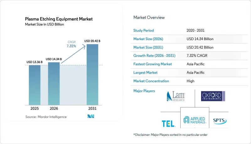
根據 Mordor Intelligence 預測,電漿蝕刻設備市場規模預計將在 2025 年達到 133.6 億美元,2026 年達到 143.4 億美元,到 2031 年達到 204.2 億美元,2026 年至 2031 年的複合年成長率為 7.32%。
本報告按類型(反應離子蝕刻、感應耦合電漿蝕刻等)、晶圓尺寸(小於150毫米、200毫米及其他)、材料(矽、化合物半導體等)、應用(家用電子電器、工業、醫療設備等)、最終用戶(鑄造等)和地區進行細分。市場預測以美元計價。
全球等電漿蝕刻設備市場趨勢及洞察
EUV微影術的擴展推動了對高深長寬比蝕刻的需求。
預計極紫外線 (EUV)微影術將於 2025 年在 3nm 節點從試驗線過渡到量產,並計劃於 2027 年在 2nm 節點全面應用。每個 EUV 步驟都要求接觸孔、通孔和閘極間隔層的長寬比超過 120:1,由於關鍵尺寸小於 10nm,因此可提高蝕刻強度。 ASML 在 2025 年第一季交付了 20 台 EUV 掃描儀,較去年同期成長 33%。每台掃描器都整合了多個感應耦合電漿(ICP) 腔室。 IBM 已成功檢驗了奈米片電晶體,該電晶體每個閘極堆疊需要 14 個獨立的蝕刻步驟,是 FinFET 節點複雜度的兩倍。因此,預計到 2025 年,蝕刻設備的資本投資將佔晶圓廠總支出的 18-22%。儀器製造商正在整合即時終點光譜功能以抑制微溝槽,而製造商正在修改其配方庫,以實現超低偏壓工藝,將側壁翹曲控制在 1 度以內。
3D NAND 和 DRAM 節點小型化進展
2024年,三星發表了一款286層垂直NAND產品。本產品需要超過15µm的蝕刻深度和小於2度的錐度,這增加了對能夠緩解長寬比延遲的深反應離子蝕刻設備的需求。 SK海力士在2025年推出的1-α奈米DRAM中採用了原子層蝕刻技術來保護高介電常數材料。同時,用於冷卻至0 度C以下的低溫製程認證正在推進,以提高氧化矽和氮化矽薄膜之間的選擇性。根據SEMI估計,2025年記憶體製造商的資本支出將達到450億美元,其中20%用於蝕刻設備。由於3D NAND層數的增加以及DRAM電容間距的小型化,預計到2031年,蝕刻步驟的數量將逐年增加。
等離子體對小於 5 nm 的結構造成的損傷
當閘極氧化層厚度接近 1 nm 時,蝕刻過程中離子碰撞導致的晶格缺陷、電荷累積和界面粗糙度會降低驅動電流並導致閾值電壓偏移。原子層蝕刻雖然可以減少損傷,但會使蝕刻週期延長三倍,增加晶圓成本。東京電子最新的原子層蝕刻平台每個週期可刻蝕 0.5 nm,但蝕刻一個 10 nm 的溝槽大約需要 200 個週期。相比之下,連續電漿蝕刻只需 30 秒即可完成。因此,此晶圓廠僅對最敏感的層進行原子層刻蝕,從而在不太關鍵的區域實現可控損傷。
細分市場分析
預計到2025年,感應耦合電漿(ICP)平台將佔據電漿蝕刻設備市場46.83%的佔有率,成為最大的貢獻者。由於離子能量和等離子體密度可以解耦,晶圓廠可以精細調節異向性,從而保護脆弱的鰭片和奈米片。預計到2031年,深反應離子(DRI)設備將以7.99%的複合年成長率成長,它對於需要20:1或更高長寬比以及50-100 µm深度的穿透矽通孔(TSV)和晶圓級封裝至關重要,因此擴大了電漿蝕刻設備在該領域的市場佔有率。雖然傳統的反應離子蝕刻設備在成熟節點上仍有需求,但其市場正逐漸轉向後緣鑄造線。
Lam Research 的「Sense.i」平台採用基於機器學習的即時偏移調整功能,預計到 2025 年,接觸孔蝕刻良率將提高約 3 個百分點。 Applied Materials 為其 Centris Sym3 增加了原位測量功能,將腔室間差異降低到 0.3 nm 以下,這對於 2 nm 環柵電晶體至關重要。隨著等離子體技術和資料科學的融合,傳統設備類別之間的界限正在變得模糊,供應商之間的競爭也日益激烈。
2025年,300毫米晶圓規格的市佔率佔比達到51.73%,支撐了等電漿蝕刻設備市場的發展。這主要得益於台積電(TSMC)、三星和英特爾等公司擁有超過50座300毫米規格的晶圓廠投入運作。隨著450毫米以上規格的先導計畫日益活躍,以及產業聯盟重新評估規模經濟效益,預計到2031年,該細分市場將以年均8.33%的速度成長。英特爾於2024年部分重啟了450毫米規格的試點項目,旨在將每片晶圓的晶片數量提高40%,以證明其預計150億美元的設備維修的合理性。
化合物半導體製造商正從150毫米和200毫米生產線轉向300毫米生產線,以降低碳化矽(SiC)和氮化鎵(GaN)裝置的單晶片成本,這進一步擴大了對300毫米設備的需求。 2025年6月,SEMI發布了化合物晶圓蝕刻均勻性和缺陷規格認證的新標準,指南供應商重新設計腔室材料以應對高腐蝕性化學品。
區域分析
預計到2025年,亞太地區將佔全球銷售額的55.72%,複合年成長率達8.66%,並將繼續保持其在電漿蝕刻設備市場的主導地位。台灣半導體產業叢集預計到2025年產值將達1,600億美元,佔全球晶圓代工廠銷售額的65%。同年,韓國將生產全球70%的DRAM和45%的NAND閃存,鞏固其作為記憶體中心的地位。受出口限制,中國正在加快引進國產設備,中芯國際(SMIC)和華虹半導體已對NAURA和先進微加工設備公司(Advanced Micro-Fabrication Equipment)的14nm和28nm製程系統進行了認證。日本正恢復投資,撥款2兆日圓(約135億美元)用於擴大國內產能,吸引了台積電(TSMC)、美光科技(Micron)和西部數據(Western Digital)等公司。
預計到2025年,北美將佔全球需求的約25%,並有望成長7.8%,這得益於《晶片法案》(CHIPS Act)的資金支持,用於在亞利桑那州、俄亥俄州、紐約州和德克薩斯州建設晶圓廠。光是英特爾位於俄亥俄州的兩座晶圓廠預計到2028年就需要超過200個蝕刻室。台積電(TSMC)計劃在2030年於亞利桑那州的工廠建成三座晶圓廠,總合能將達到60萬片晶圓,所有晶圓廠都將配備最先進的等離子切割系統。
根據預測,歐洲在2025年將佔據全球半導體市場約10%的佔有率,但根據歐盟《晶片法案》430億歐元的撥款,其目標是在2030年佔據全球半導體產量的20%。英特爾的馬德堡計畫、意法半導體和格羅方德在法國的合資工廠以及英飛凌的德勒斯登擴建計劃,都已宣布投資超過800億歐元(約870億美元)。中東和非洲仍處於規劃階段,阿布達比和利雅德正在建造設計和封裝設施。南美洲的活動僅限於巴西和阿根廷的組裝業務,而澳洲和紐西蘭雖然參與了調查,但並未進行大規模生產。
其他好處:
- Excel格式的市場預測(ME)表
- 3個月的分析師支持
目錄
第1章:引言
- 研究假設和市場定義
- 調查範圍
第2章:調查方法
第3章執行摘要
第4章 市場狀況
- 市場概覽
- 市場促進因素
- EUV微影術的擴展推動了對高深長寬比蝕刻的需求。
- 3D NAND 的普及和 DRAM 的小型化
- 對化合物半導體功率元件的需求不斷成長
- 政府主導的半導體自給自足計畫(美國 CHIPS 法案、歐盟 CHIPS 法案)
- 向異構整合和先進封裝的過渡
- 量子計算設備製造領域的新應用
- 市場限制因素
- 等離子體對小於 5 nm 的結構造成的損傷
- 潔淨室的建設成本和運作成本都在飆升。
- 高純度特種氣體供應鏈的波動
- 智慧財產權法規限制設備出口到中國。
- 價值鏈分析
- 監理情勢
- 技術展望
- 波特五力分析
- 宏觀經濟因素影響評估
第5章 市場規模與成長預測
- 按類型
- 反應離子蝕刻(RIE)
- 感應耦合電漿蝕刻(ICP)
- 深反應離子蝕刻(DRIE)
- 高密度電漿蝕刻(HDPE)
- 其他類型
- 按晶圓尺寸
- 小於150毫米
- 200 mm
- 300 mm
- 450毫米或以上
- 材料
- 矽
- 化合物半導體
- 玻璃和聚合物
- 其他材料
- 透過使用
- 家用電子產品
- 產業
- 醫療器材
- 汽車電子
- 航太/國防
- 其他用途
- 最終用戶
- 鑄造廠
- 垂直整合設備製造商(IDM)
- 研究和學術機構
- 其他最終用戶
- 按地區
- 北美洲
- 美國
- 加拿大
- 墨西哥
- 南美洲
- 巴西
- 阿根廷
- 其他南美國家
- 歐洲
- 英國
- 德國
- 法國
- 義大利
- 西班牙
- 其他歐洲國家
- 亞太地區
- 中國
- 日本
- 印度
- 韓國
- 澳洲和紐西蘭
- 其他亞太國家
- 中東和非洲
- 中東
- 沙烏地阿拉伯
- 阿拉伯聯合大公國
- 土耳其
- 其他中東國家
- 非洲
- 南非
- 奈及利亞
- 其他非洲國家
- 中東
- 北美洲
第6章 競爭情勢
- 市場集中度
- 策略趨勢
- 市佔率分析
- 公司簡介
- Applied Materials Inc.
- Lam Research Corporation
- Tokyo Electron Limited
- Hitachi High-Tech Corporation
- KLA-SPTS Technologies
- Oxford Instruments plc
- Advanced Micro-Fabrication Equipment Inc.(AMEC)
- NAURA Technology Group Co. Ltd.
- Plasma-Therm LLC
- Samco Inc.
- ULVAC Inc.
- Plasma Etch Inc.
- Sentech Instruments GmbH
- GigaLane Co. Ltd.
- Thierry Corporation
- Panasonic Factory Solutions Co.
- TRION Technology Inc.
- Veeco Instruments Inc.
- Mattson Technology Inc.
- CORIAL
第7章 市場機會與未來展望
According to Mordor Intelligence, the plasma etching equipment market size is projected to be USD 13.36 billion in 2025, USD 14.34 billion in 2026, and reach USD 20.42 billion by 2031, growing at a CAGR of 7.32% from 2026 to 2031.
This report is Segmented by Type (Reactive Ion Etching, Inductively Coupled Plasma Etching, and More), Wafer Size (Below 150 Mm, 200 Mm, and More), Material (Silicon, Compound Semiconductors, and More), Application (Consumer Electronics, Industrial, Medical Devices, and More), End User (Foundries, and More), and Geography. The Market Forecasts are Provided in Terms of Value (USD).
Global Plasma Etching Equipment Market Trends and Insights
Expansion of EUV Lithography Driving High Aspect-Ratio Etch Requirements
Extreme ultraviolet lithography transitioned from pilot lines to high-volume manufacturing at the 3 nm node in 2025 and is slated for adoption at the 2 nm node by 2027. Each EUV step increases etch intensity because contact holes, vias, and gate spacers now require aspect ratios exceeding 120:1, with critical dimensions below 10 nm. ASML shipped 20 EUV scanners in Q1 2025, a 33% year-over-year increase, and every scanner is paired with multiple inductively coupled plasma chambers. IBM validated nanosheet transistors that require 14 separate etch steps per gate stack, doubling complexity over finFET nodes. Capital outlays for etch tools consequently rose to 18-22% of total fab spending in 2025. Tool makers are embedding real-time endpoint spectroscopy to suppress micro-trenching, and fabs are revising recipe libraries to execute ultra-low bias processes that cut sidewall bowing to within 1 degree.
Proliferation of 3D NAND and DRAM Node Shrinks
Samsung disclosed a 286-layer vertical NAND product in 2024 that necessitates etch depths exceeding 15 µm with sub-2-degree taper, magnifying demand for deep reactive ion equipment calibrated to mitigate aspect-ratio-dependent lag. SK Hynix adopted atomic layer etching to protect high-k dielectrics in its 1-alpha-nm DRAM, launched in 2025. Meanwhile, cryogenic processes cooled below 0 °C are being qualified to improve selectivity between silicon oxide and nitride. SEMI estimated memory companies spent USD 45 billion on capital equipment in 2025, 20% of which was devoted to etch platforms. High layer counts in 3D NAND and shrinking capacitor pitches in DRAM will keep etch process steps rising each year through 2031.
Plasma-Induced Damage in Sub-5 nm Structures
Lattice defects, charge accumulation, and interface roughness caused by ion bombardment during etch steps cut drive current and shift threshold voltage when the gate oxide thickness approaches 1 nm. Atomic layer etching reduces damage but triples the cycle time, thereby increasing the cost per wafer. Tokyo Electron's latest atomic layer platform removes 0.5 nm per cycle but requires approximately 200 cycles to clear a 10 nm trench, compared to 30 seconds for a continuous plasma etch. Fabs are therefore limiting atomic layer methods to the most sensitive layers while accepting controlled damage in less critical regions.
Other drivers and restraints analyzed in the detailed report include:
- Growing Demand for Compound-Semiconductor Power Devices
- Government-Backed Chip Sovereignty Programs
- Rising Clean-Room Construction and Utility Costs
For complete list of drivers and restraints, kindly check the Table Of Contents.
Segment Analysis
Inductively coupled plasma platforms generated the largest plasma etching equipment market size contribution at 46.83% in 2025. Their capacity to decouple ion energy from plasma density lets fabs fine-tune anisotropy and protect fragile fins and nanosheets. Deep reactive ion equipment, projected to grow at a 7.99% CAGR through 2031, is key for through-silicon vias and wafer-level packaging that require depths of 50-100 µm at aspect ratios of greater than 20:1, thereby expanding the plasma etching equipment market share held by this segment. Conventional reactive ion tools remain in demand at mature nodes but are gradually migrating toward trailing-edge foundry lines.
Lam Research's Sense.i platform employs machine learning for real-time bias adjustments that have raised yield by roughly 3 percentage points in contact-hole etch since 2025. Applied Materials added in-situ metrology to its Centris Sym3 to cut chamber-to-chamber variation below 0.3 nm, a necessity for 2 nm gate-all-around transistors. This convergence of plasma and data science is blurring legacy boundaries between tool categories and intensifying supplier competition.
The 300 mm format accounted for 51.73% of 2025 demand, anchoring the plasma etching equipment market size because Taiwan Semiconductor Manufacturing Company, Samsung, and Intel collectively ran more than 50 fabs on this diameter. Above-450 mm pilot work is picking up, and the segment is predicted to grow at 8.33% through 2031 as industry consortia revisit economies of scale. Intel restarted limited 450 mm pathfinding in 2024, seeking a 40% die-count boost per wafer to justify a projected USD 15 billion retrofit.
Compound-semiconductor makers are shifting from 150 mm and 200 mm to 300 mm lines to cut cost per die in silicon carbide and gallium nitride devices, further enlarging 300 mm tool requirements. SEMI released updated standards in June 2025 to certify etch uniformity and defect specifications for compound wafers, guiding suppliers in redesigning chamber materials for corrosive chemistries.
Complete Report Scope:
- By Type
- Reactive Ion Etching (RIE)
- Inductively Coupled Plasma Etching (ICP)
- Deep Reactive Ion Etching (DRIE)
- High Density Plasma Etching (HDPE)
- Other Types
- By Wafer Size
- Below 150 mm
- 200 mm
- 300 mm
- Above 450 mm
- By Material
- Silicon
- Compound Semiconductors
- Glass and Polymers
- Other Materials
- By Application
- Consumer Electronics
- Industrial
- Medical Devices
- Automotive Electronics
- Aerospace and Defense
- Other Applications
- By End User
- Foundries
- Integrated Device Manufacturers (IDMs)
- Research and Academic Institutions
- Other End Users
- By Geography
- North America
- United States
- Canada
- Mexico
- South America
- Brazil
- Argentina
- Rest of South America
- Europe
- United Kingdom
- Germany
- France
- Italy
- Spain
- Rest of Europe
- Asia-Pacific
- China
- Japan
- India
- South Korea
- Australia and New Zealand
- Rest of Asia Pacific
- Middle East and Africa
- Middle East
- Saudi Arabia
- United Arab Emirates
- Turkey
- Rest of Middle East
- Africa
- South Africa
- Nigeria
- Rest of Africa
- Middle East
- North America
Geography Analysis
The Asia-Pacific region generated 55.72% of the revenue in 2025 and is projected to achieve an 8.66% CAGR, ensuring it continues to dominate the plasma etching equipment market. Taiwan's cluster yielded USD 160 billion output in 2025, 65% of global foundry revenue. South Korea produced 70% of DRAM and 45% of NAND that year, cementing its position as the memory hub. China, constrained by export controls, accelerated the uptake of domestic tools, with Semiconductor Manufacturing International Corporation and Hua Hong Semiconductor qualifying NAURA and Advanced Micro-Fabrication Equipment systems for 14 nm and 28 nm flows. Japan reignited investment by allocating JPY 2 trillion (USD 13.5 billion) for local capacity, attracting Taiwan Semiconductor Manufacturing Company, Micron, and Western Digital.
North America represented roughly 25% of 2025 demand and is projected to grow 7.8% as CHIPS Act funds underwrite fabs in Arizona, Ohio, New York, and Texas. Intel's two-fab Ohio campus alone is expected to need more than 200 etch chambers by 2028. Taiwan Semiconductor Manufacturing Company's Arizona complex will host three fabs with combined capacity of 600,000 wafer starts per year by 2030, all equipped with leading-edge plasma tools.
Europe held about 10% share in 2025 but is aiming to capture 20% of global chip output by 2030 under the EUR 43 billion EU Chips Act allocation. Intel's Magdeburg project, STMicroelectronics-GlobalFoundries' French joint facility, and Infineon's Dresden expansion represent more than EUR 80 billion (USD 87 billion) in announced investments. Middle East and Africa remain in the exploratory phase, with Abu Dhabi and Riyadh pursuing design and packaging hubs. South America's activity is limited to assembly initiatives in Brazil and Argentina, while Australia and New Zealand contribute research but not large-scale fabrication.
- Applied Materials Inc.
- Lam Research Corporation
- Tokyo Electron Limited
- Hitachi High-Tech Corporation
- KLA - SPTS Technologies
- Oxford Instruments plc
- Advanced Micro-Fabrication Equipment Inc. (AMEC)
- NAURA Technology Group Co. Ltd.
- Plasma-Therm LLC
- Samco Inc.
- ULVAC Inc.
- Plasma Etch Inc.
- Sentech Instruments GmbH
- GigaLane Co. Ltd.
- Thierry Corporation
- Panasonic Factory Solutions Co.
- TRION Technology Inc.
- Veeco Instruments Inc.
- Mattson Technology Inc.
- CORIAL
Additional Benefits:
- The market estimate (ME) sheet in Excel format
- 3 months of analyst support
TABLE OF CONTENTS
1 INTRODUCTION
- 1.1 Study Assumptions and Market Definition
- 1.2 Scope of the Study
2 RESEARCH METHODOLOGY
3 EXECUTIVE SUMMARY
4 MARKET LANDSCAPE
- 4.1 Market Overview
- 4.2 Market Drivers
- 4.2.1 Expansion of EUV Lithography Driving High Aspect-Ratio Etch Requirements
- 4.2.2 Proliferation of 3D NAND and DRAM Node Shrinks
- 4.2.3 Growing Demand for Compound-Semiconductor Power Devices
- 4.2.4 Government-Backed Chip Sovereignty Programs (US CHIPS Act, EU Chips Act)
- 4.2.5 Shift Toward Heterogeneous Integration and Advanced Packaging
- 4.2.6 Emerging Use in Quantum Computing Device Fabrication
- 4.3 Market Restraints
- 4.3.1 Plasma-Induced Damage in Sub-5 nm Structures
- 4.3.2 Rising Clean-Room Construction and Utility Costs
- 4.3.3 Supply Chain Volatility for High-Purity Specialty Gases
- 4.3.4 IP Restrictions Limiting Equipment Exports to China
- 4.4 Value Chain Analysis
- 4.5 Regulatory Landscape
- 4.6 Technological Outlook
- 4.7 Porter's Five Forces Analysis
- 4.7.1 Bargaining Power of Suppliers
- 4.7.2 Bargaining Power of Consumers
- 4.7.3 Threat of New Entrants
- 4.7.4 Threat of Substitutes
- 4.7.5 Intensity of Competitive Rivalry
- 4.8 Assessment of Impact of Macroeconomic Factors
5 MARKET SIZE AND GROWTH FORECASTS (VALUE)
- 5.1 By Type
- 5.1.1 Reactive Ion Etching (RIE)
- 5.1.2 Inductively Coupled Plasma Etching (ICP)
- 5.1.3 Deep Reactive Ion Etching (DRIE)
- 5.1.4 High Density Plasma Etching (HDPE)
- 5.1.5 Other Types
- 5.2 By Wafer Size
- 5.2.1 Below 150 mm
- 5.2.2 200 mm
- 5.2.3 300 mm
- 5.2.4 Above 450 mm
- 5.3 By Material
- 5.3.1 Silicon
- 5.3.2 Compound Semiconductors
- 5.3.3 Glass and Polymers
- 5.3.4 Other Materials
- 5.4 By Application
- 5.4.1 Consumer Electronics
- 5.4.2 Industrial
- 5.4.3 Medical Devices
- 5.4.4 Automotive Electronics
- 5.4.5 Aerospace and Defense
- 5.4.6 Other Applications
- 5.5 By End User
- 5.5.1 Foundries
- 5.5.2 Integrated Device Manufacturers (IDMs)
- 5.5.3 Research and Academic Institutions
- 5.5.4 Other End Users
- 5.6 By Geography
- 5.6.1 North America
- 5.6.1.1 United States
- 5.6.1.2 Canada
- 5.6.1.3 Mexico
- 5.6.2 South America
- 5.6.2.1 Brazil
- 5.6.2.2 Argentina
- 5.6.2.3 Rest of South America
- 5.6.3 Europe
- 5.6.3.1 United Kingdom
- 5.6.3.2 Germany
- 5.6.3.3 France
- 5.6.3.4 Italy
- 5.6.3.5 Spain
- 5.6.3.6 Rest of Europe
- 5.6.4 Asia-Pacific
- 5.6.4.1 China
- 5.6.4.2 Japan
- 5.6.4.3 India
- 5.6.4.4 South Korea
- 5.6.4.5 Australia and New Zealand
- 5.6.4.6 Rest of Asia Pacific
- 5.6.5 Middle East and Africa
- 5.6.5.1 Middle East
- 5.6.5.1.1 Saudi Arabia
- 5.6.5.1.2 United Arab Emirates
- 5.6.5.1.3 Turkey
- 5.6.5.1.4 Rest of Middle East
- 5.6.5.2 Africa
- 5.6.5.2.1 South Africa
- 5.6.5.2.2 Nigeria
- 5.6.5.2.3 Rest of Africa
- 5.6.5.1 Middle East
- 5.6.1 North America
6 COMPETITIVE LANDSCAPE
- 6.1 Market Concentration
- 6.2 Strategic Moves
- 6.3 Market Share Analysis
- 6.4 Company Profiles (includes Global-level Overview, Market-level Overview, Core Segments, Financials as available, Strategic Information, Market Rank/Share, Products and Services, Recent Developments)
- 6.4.1 Applied Materials Inc.
- 6.4.2 Lam Research Corporation
- 6.4.3 Tokyo Electron Limited
- 6.4.4 Hitachi High-Tech Corporation
- 6.4.5 KLA - SPTS Technologies
- 6.4.6 Oxford Instruments plc
- 6.4.7 Advanced Micro-Fabrication Equipment Inc. (AMEC)
- 6.4.8 NAURA Technology Group Co. Ltd.
- 6.4.9 Plasma-Therm LLC
- 6.4.10 Samco Inc.
- 6.4.11 ULVAC Inc.
- 6.4.12 Plasma Etch Inc.
- 6.4.13 Sentech Instruments GmbH
- 6.4.14 GigaLane Co. Ltd.
- 6.4.15 Thierry Corporation
- 6.4.16 Panasonic Factory Solutions Co.
- 6.4.17 TRION Technology Inc.
- 6.4.18 Veeco Instruments Inc.
- 6.4.19 Mattson Technology Inc.
- 6.4.20 CORIAL
7 MARKET OPPORTUNITIES AND FUTURE OUTLOOK
- 7.1 White-Space and Unmet-Need Assessment


