|
市場調查報告書
商品編碼
1548963
混合加入:專利格局分析(2024)Hybrid Bonding - Patent Landscape Analysis 2024 |
|||||||
主要功能
- 70+ PDF 投影片
- Excel 文件:1,600 多 專利族
- 全球專利趨勢:專利公佈、專利申請國家等的時間趨勢。
- 每個細分市場的主要專利權人和新進者。
- 主要公司的智慧財產權地位及其專利組合的相對實力。
- 依發明類型(製造方法、裝置、半導體結構和裝置)和目標應用(影像感測器、2.5D/3D IC、3D 堆疊記憶體、光子學等)分類的專利。
- 主要公司的智慧財產權概況(專利組合概覽、技術覆蓋範圍、地理覆蓋範圍、關鍵專利、近期智慧財產權活動等)
- 包含報告中分析的所有專利的 Excel 資料庫(專利分類、更新線上資料庫的超連結、受讓人從統計分析中獲得的所有資料)。
在決定半導體封裝未來的尖端鍵結技術的全球 IP 競爭市場中,誰是主要參與者和新進者?
混合鍵結是先進封裝的關鍵
混合鍵結結合了電介質對電介質鍵合和金屬對金屬鍵合,可在不使用焊料或其他黏合劑的情況下互連晶圓到晶圓、晶片到晶圓以及晶片到晶片。這種鍵合技術用於多個晶片的垂直堆疊,允許在一個封裝內實現具有各種功能(邏輯、記憶體、類比、感測器等)的不同類型晶片的 3D 異構整合和互通性。混合結可實現細間距(小於10微米,甚至小於1微米),這在互連密度和裝置性能方面具有顯著優勢。金屬與金屬的直接接觸可促進高效散熱並減少寄生延遲。由於電介質使每個金屬焊盤絕緣,因此焊盤之間不存在訊號幹擾。
混合鍵結技術於 2005 年隨著 Ziptronix 的 DBI-R(直接鍵結互連)技術的推出而出現。 2015年,Tessera(現為Adeia)收購了Ziptronix,DBI-R技術於2016年透過索尼的CMOS影像感測器(CIS)進入市場,該技術應用於三星Galaxy S7手機。從那時起,混合鍵合技術在記憶體、邏輯、射頻和光子學等各種應用中得到了探索,現在被半導體行業的更多公司採用。
在過去五年中,混合鍵結技術已成為先進半導體封裝的關鍵推動因素,導致專利活動增加和競爭性智??慧財產權 (IP) 格局的重大演變。主要專利持有者正在加強在美國、中國和歐洲的智慧財產權地位,同時各種新公司正在進入專利領域。目前,對於半導體封裝產業的企業來說,從智慧財產權的角度審視混合鍵結技術極為重要。
在此背景下,Knowmade 正在分析新的專利格局,重點在於使用混合鍵合製程和混合鍵結互連的半導體裝置。從 1,600 多個專利族(發明)中提取了 5,800 多項專利。本報告的目的是深入了解當前的智慧財產權活動、領先的智慧財產權公司的地位、其專利的目標開發領域以及其專利組合如何支持其市場策略。
主要趨勢、主要企業智慧財產權地位及智慧財產權策略分析
透過專利分析,我們解釋智慧財產權 (IP) 公司的地位,揭示加強其智慧財產權組合的策略,強調其限制其他公司的專利活動和營運自由的能力,並識別有前途的新公司。未來的知識產權領導者。 IP 競爭分析必須反映具有進入和擴展先進半導體封裝市場策略的公司的願景。本報告全面概??述了競爭性智慧財產權格局以及與混合鍵結技術相關的最新技術發展。該報告涵蓋智慧財產權動態和主要趨勢,包括專利申請、專利受讓人、申請國家、專利技術和涵蓋的申請。我們還確定了知識產權領導者和最活躍的專利申請人,並重點關注該領域的未知公司和新進入者。
發明類型、目標申請、主要專利
專利涵蓋了所要求的發明類型(混合結製造方法和介面工程、混合結技術設備、混合結半導體結構/裝置)以及專利中提到的應用(影像感測器、2.5D/3D IC、 3D 堆疊記憶體、光子學、MEMS、RF 等)。目前,2.5D/3D IC 領域正在推動專利活動,但與光子學、micro-LED、MEMS 和 RF 等其他活動相關的專利正在迅速增加。
動態智慧財產權格局:領先公司地位的演變與新專利申請人的進入
台積電、Adeia、長江儲存、英特爾、三星引領專利情勢,活躍專利活動,擴大主要國家的發明保護。 Adeia 是 DBI-R 技術的先驅和所有者,採取了積極的策略,向索尼、長江存儲、美光和 Kioxia 等多家半導體公司申請專利並將其混合結 IP 組合授權。儘管該公司擁有強大的智慧財產權地位,但其他公司正在開發自己的混合黏合專利組合。近年來,越來越多的記憶體製造商涉足IP環境(CXMT、SK Hynix、Sunrise Memory),OSAT和設備/材料供應商也進入IP領域(ASE、TongFu、SJSemi、Applied Materials)。 。本報告概述了主要公司持有的智慧財產權組合,並描述了他們的關鍵專利和最近的智慧財產權活動。此外,我們也涵蓋主要智慧財產權合作(共同擁有專利、智慧財產權轉讓、授權協議)和專利訴訟。
有用的 Excel 專利資料庫
報告包括專利資訊(編號、日期、受讓人、標題、摘要等)、更新線上資料庫的超連結(文字、法律狀態等)、隸屬關係部分(製造方法、設備、包含廣泛的 Excel包含本報告分析的所有專利(包括半導體裝置、影像感測器、2.5D/3D IC、3D堆疊記憶體等)和關鍵專利的資料庫。此外,Excel 文件還包含受讓人從統計分析中獲得的完整信息,包括專利族數量、專利活動時間表、已授權和待審專利數量以及專利組合的區域分析數據。
本報告提及的企業 (部分)
TSMC,YMTC,Xperi/Adeia,Intel,Samsung,XMC,Micron,Tongfu Microelectronics,ASE,Meta (Facebook),Nanya Technology,CXMT,Huawei,Onsemi,OmniVision,AMD,ICLeague Technology,Monolithic 3D,UMC/Wavetek,Qualcomm,SJSemi,Saultech,SK Hynix,Tsinghua University,CEA,imec,Galaxycore Microelectronics,Apple,EVG,HD MicroSystems,NCAP,STMicroelectronics,Applied Materials,Resonac,GlobalFoundries,SunRise Memory,阿里巴巴 Group,AP Memory,SMIC,Powerchip Semiconductor Manufacturing,MICLEDI,AMS-Osram,SmartSens Technology,深圳 Aoshiwei Technology,MediaTek,IBM,RTX Corporation,pSemi,Winbond electronics,Sony,NVIDIA,Haiguang Information Technology,Shanghai Huali Integrated Circuit Manufacturing,JCET Group,SEMES,Tectus Group,Hanmi,Western Digital,Shibaura Mechatronics,寧波 Semiconductor International Corporation (NSI),HIDM - Huaian Imaging Device Manufacturer,Bruker,Suzhou Ultiview Technology,KLA,Shanghai Fudan Microelectronics Group,Anhui Xinbiyou Information Technology,Tokyo Electron,Shanghai Yibu Semiconductor,HTSI,GROQ,Dixtech innovation,Qingdao New Core Technology,PsiQuantum,Canon,Infineon,Shanghai Biren Intelligent Technology,Yangtze River Advanced Storage Industry Innovation Center,G-ray Switzerland等。
目錄
簡介
摘要整理
Excel資料庫
- 含由於從為了本報告被選擇了的全部的專利和,統計分析被得了的受讓人的完全的資料的Excel文件
專利形勢概要
- 主要趨勢和IP企業
- 專利出版數量的時間序列變化
- 主要專利權人
- 知識產權公司時間表
- 知識產權公司的主要類型
- 知識產權領域的新進入者
- 主要公司的專利:當前法律狀況
- 專利權人的智慧財產權領先地位以及 2019 年以來的演變
- 主要公司專利的地理範圍
- 主要的IP合作
- 共同所有IP
- IP轉讓
- 授權合約
- 專利的市場區隔
- 市場區隔定義
- 要求保護的發明類型:
- 混合連接製造流程和介面工程
- 混合鍵結設備
- 使用混合結互連製造的半導體結構/裝置
- 目標用途
- 影像感測器(SPAD、CMOS影像感測器、光學感測器等)
- D/3D IC(任何類型 IC 晶片的組裝(內存對內存除外))
- 3D堆疊記憶體(記憶體上的記憶體)
- 其他應用(射頻、MEMS、光子學、LED 等)
- 專利出版數量趨勢:按細分市場
- 主要專利權人:依細分市場劃分
- 專利權人的智慧財產權領導力:每個細分市場
主要專利
- 從現有技術、智慧財產權風險和技術角度來看最重要的專利
- 主要專利屬於的市場區隔
- 主要專利的所有者
發明專利權者選擇的IP簡介
- TSMC,Adeia/Xperi,TongFu,ASE
- 各企業相關:
- 專利組合概要 (IP動態,市場區隔,法律上的狀態,企業發展地區等)
- 主要專利的說明
- 最近的專利申請的說明
專利訴訟
附錄
KNOWMADE的簡報
KEY FEATURES:
- PDF>70 slides
- Excel file>1,600 patent families
- Global patenting trends, including time evolution of patent publications, countries of patent filings, etc.
- Main patent assignees and IP newcomers in the different segments.
- Key players' IP position and the relative strength of their patent portfolio.
- Patents categorized by type of invention (manufacturing methods, equipment, semiconductor structures and devices) and targeted applications (image sensors, 2.5D/3D IC, 3D-stacked memories, photonics, etc.)
- IP profile of key players (patent portfolio overview, technical coverage, geographical coverage, key patents, recent IP activity, etc.)
- Excel database containing all patents analyzed in the report, including patent segmentations and hyperlinks to an updated online database, along with the complete data by assignee from the statistical analyses.
Who are the key players and newcomers in the global IP race for the most advanced bonding technology shaping the future of semiconductor packaging?
Hybrid bonding has become a key enabler of advanced packaging
Hybrid bonding combines dielectric-to-dielectric and metal-to-metal bonds to interconnect wafer-to-wafer, die-to-wafer, or die-to-die without the need for solder or other adhesives. This bonding technology is used for the vertical stacking of multiple chips, enabling 3D heterogeneous integration and interoperability of different types of chips with various functions (e.g., logic, memory, analog, sensors) within a single package. Hybrid bonding enables finer pitch (<10 micrometerm, or even <1 micrometerm) with significant benefits for interconnect density and device performance. The direct metal-to-metal contact facilitates efficient heat dissipation and reduces the parasitic delay. The dielectric insulates each metal pad so that there is no signal interference between the pads.
Hybrid bonding technology emerged in 2005 with the introduction of Ziptronix's direct bond interconnect (DBI-R) technology. In 2015, Tessera (now Adeia) acquired Ziptronix, and DBI-R technology entered the market in 2016 through Sony's CMOS image sensor (CIS) used in Samsung's Galaxy S7 mobile phone. Since then, hybrid bonding technology has been explored for various applications, including memory, logic, RF, and photonics, and it is now being adopted by more companies across the semiconductor industry.
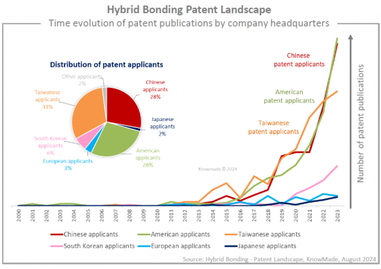
Over the past five years, hybrid bonding technology has become a key enabler of advanced semiconductor packaging, leading to a strong increase in patenting activity and a significant evolution of the competitive intellectual property (IP) landscape. Major patent owners have strengthened their IP positions in the US, China, and Europe, while various new players have entered the patent landscape. It is now crucial for companies operating in the semiconductor packaging industry to closely examine hybrid bonding technology from an IP perspective.
In this context, Knowmade is releasing a new patent landscape report focusing on the hybrid bonding process and semiconductor devices made using hybrid bonding interconnects. Over 5,800 patents from more than 1,600 patent families (inventions) have been selected. This report aims to provide insights into current IP activities, the positions of key IP players, the applications they target in their patents, and how their patent portfolios can support their market strategies.

Understanding the main trends, the key players' IP position and IP strategy
Through patent analysis, we describe the position of IP players, unveil their strategies to strengthen their IP portfolio, highlight their capability to limit the patenting activity and freedom-to-operate of other firms, identify promising new players, and forecast what would be the future IP leaders. IP competition analysis should reflect the vision of players with a strategy to enter and develop their business in the advanced semiconductor packaging market. In this report, we provide a comprehensive overview of the competitive IP landscape and latest technological developments related to hybrid bonding technology. The report covers IP dynamics and key trends in terms of patents applications, patent assignees, filing countries, patented technologies, and targeted applications. It also identifies the IP leaders, most active patent applicants, and sheds light on under-the-radar companies and new players in this field.
Invention type, targeted applications, and key patents
The patents have been categorized according to the type of claimed invention (hybrid bonding manufacturing methods and interface engineering, equipment for hybrid bonding technology, hybrid bonded semiconductor structures or devices) and the applications mentioned in the patents (image sensors, 2.5D/3D ICs, 3D-stacked memories, photonics, MEMS, RF, etc.). The 2.5D/3D IC segment is currently driving patenting activity, while patents related to other applications, such as photonics, microLED, MEMS, and RF, have surged.

A dynamic IP landscape: evolution of leading players' positions and entry of new patent applicants
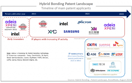
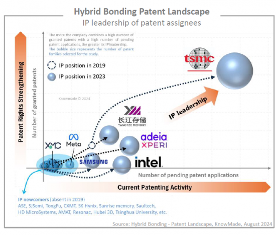
TSMC, Adeia, YMTC, Intel, and Samsung are leading the patent landscape, increasing patenting activity, and expanding invention protection in key countries. As pioneer and owner of DBI-R technology, Adeia has adopted an aggressive strategy to assert its patents and license its hybrid bonding IP portfolio to various semiconductor companies, including Sony, YMTC, Micron, and Kioxia. Despite its strong IP position, other players have been developing their own hybrid bonding patent portfolios. In recent years, more memory makers have become involved in the IP landscape (CXMT, SK Hynix, Sunrise Memory), and OSATs and equipment/materials suppliers have entered the IP arena (ASE, TongFu, SJSemi, Applied Materials, Saultech, HD MicroSystems). In this report, we provide an overview of the IP portfolios held by key players and describe key patents and recent IP activities. Additionally, we highlight the main IP collaborations (co-owned patents, IP transfers, licensing agreements) and patent litigations.

Useful Excel patent database
This report includes an extensive Excel database with all patents analyzed in this study, including patent information (numbers, dates, assignees, title, abstract, etc.) and hyperlinks to an updated online database (original documents, legal status, etc.), affiliation segments (manufacturing methods, equipment, semiconductor devices, image sensors, 2.5D/3D IC, 3D-stacked memory, etc.), and key patents. Additionally, the Excel file comprises the complete data by assignee from the statistical analyses, including the number of patent families, timeline of patenting activity, number of granted patents and pending patent applications, and geographical coverage of patent portfolio.
Companies mentioned in the report (non-exhaustive)
TSMC, YMTC, Xperi/Adeia, Intel, Samsung, XMC, Micron, Tongfu Microelectronics, ASE, Meta (Facebook), Nanya Technology, CXMT, Huawei, Onsemi, OmniVision, AMD, ICLeague Technology, Monolithic 3D, UMC/Wavetek, Qualcomm, SJSemi, Saultech, SK Hynix, Tsinghua University, CEA, imec, Galaxycore Microelectronics, Apple, EVG, HD MicroSystems, NCAP, STMicroelectronics, Applied Materials, Resonac, GlobalFoundries, SunRise Memory, Alibaba Group, AP Memory, SMIC, Powerchip Semiconductor Manufacturing, MICLEDI, AMS-Osram, SmartSens Technology, Shenzhen Aoshiwei Technology, MediaTek, IBM, RTX Corporation, pSemi, Winbond electronics, Sony, NVIDIA, Haiguang Information Technology, Shanghai Huali Integrated Circuit Manufacturing, JCET Group, SEMES, Tectus Group, Hanmi, Western Digital, Shibaura Mechatronics, Ningbo Semiconductor International Corporation (NSI), HIDM - Huaian Imaging Device Manufacturer, Bruker, Suzhou Ultiview Technology, KLA, Shanghai Fudan Microelectronics Group, Anhui Xinbiyou Information Technology, Tokyo Electron, Shanghai Yibu Semiconductor, HTSI, GROQ, Dixtech innovation, Qingdao New Core Technology, PsiQuantum, Canon, Infineon, Shanghai Biren Intelligent Technology, Yangtze River Advanced Storage Industry Innovation Center, G-ray Switzerland, and more.
TABLE OF CONTENTS
INTRODUCTION
- Context and objectives of the report
- Scope of the report
- Reading guide
- Excel database
EXECUTIVE SUMMARY
EXCEL DATABASE
- Excel file that includes all patent selected for this study, along with the
- complete data by assignee from the statistical analyses.
PATENT LANDSCAPE OVERVIEW
- Main trends and IP players
- Time evolution of patent publications
- Main patent assignees
- Timeline of IP players
- Typology of main IP players
- IP newcomers
- Current legal status of main players' patents
- IP leadership of patent assignees and evolution from 2019
- Geographical coverage of main players' patents
- Main IP collaborations
- Co-owned IP
- IP transfers
- Licensing agreements
- Patent segmentation
- Segments definition
- Type of claimed invention:
- Hybrid bonding manufacturing process and interface engineering
- Apparatus/Equipment for hybrid bonding
- Semiconductor structure or device made using hybrid bonding interconnects
- Targeted applications
- Image sensor (SPADs, CMOS image sensors, light sensing devices, etc.)
- 2.5D/3D IC (assembly of any type of IC dies, excluding memory-on-memory)
- 3D-stacked memory (memory-on-memory)
- Other applications (RF, MEMS, Photonics, LEDs, etc.)
- Time evolution of patent publication by segment
- Main patent assignees by segment
- IP leadership of patent assignees for each segment
KEY PATENTS
- Most important patents in terms of prior-art, IP risks and technology
- Segments to which key patents belong
- Owners of key patents
IP PROFILE OF A SELECTION OF PATENT ASSIGNEES
- TSMC, Adeia/Xperi, TongFu, ASE
- For each player:
- Patent portfolio overview (IP dynamics, segments, legal status, geographic coverage, etc.)
- Description of key patents
- Description of recent patent applications
PATENT LITIGATION
ANNEX
- Methodology for patent search, selection and analysis
- Methodology to identify key patents
- Terminology


