


 |
市場調查報告書
商品編碼
1851280
先進封裝:市場佔有率分析、行業趨勢、統計數據和成長預測(2025-2030 年)Advanced Packaging - Market Share Analysis, Industry Trends & Statistics, Growth Forecasts (2025 - 2030) |
||||||
※ 本網頁內容可能與最新版本有所差異。詳細情況請與我們聯繫。
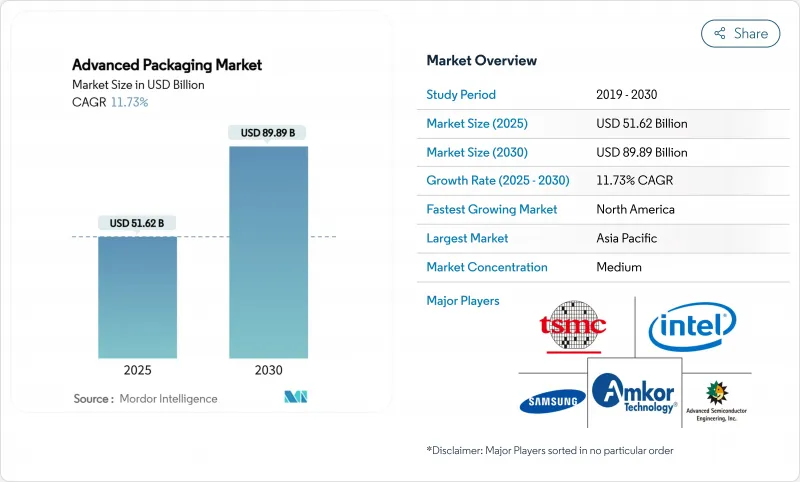
預計到 2025 年,先進封裝市場規模將達到 516.2 億美元,到 2030 年將達到 898.9 億美元,年複合成長率為 11.73%。
由於異質整合對於人工智慧 (AI) 處理器至關重要,而傳統封裝的散熱和互連能力又受到限制,因此市場需求超出了先前的預期。這促使整合設備製造商 (IDM) 和半導體組裝測試外包 (OSAT) 服務商加快資本支出,同時各國政府也累計了多項激勵措施,鼓勵本地化組裝能力。先進封裝市場也受惠於玻璃芯基板的研發、面板級加工試驗以及超大規模資料中心對共封裝光學元件的快速應用。然而,供應仍然緊張,BT 樹脂基板短缺和工程人才匱乏阻礙了產能的及時提升。隨著代工廠將封裝業務納入內部,以管理端到端的 AI 供應鏈,競爭日益激烈,傳統 OSAT 服務商的利潤空間被壓縮,策略專業化趨勢也隨之興起。
全球先進封裝市場趨勢與洞察
人工智慧和高效能運算對異質整合的需求日益成長
人工智慧工作負載需要傳統封裝無法實現的運算密度和記憶體頻寬。台積電的CoWoS平台將晶片組和高頻寬記憶體整合到單一結構中,並正迅速被主流人工智慧加速器廠商所採用。三星的SAINT技術採用混合鍵結技術實現了類似的目標,並支援即將推出的HBM4堆疊,凸顯了自主研發先進封裝的戰略價值。導熱介面材料、專用基板和主動中介層等技術的出現,使得封裝成本佔半導體總成本的比例從主流CPU的5%-8%上升至15%-20%。因此,先進封裝產能對於人工智慧系統的上市時間而言,其重要性堪比尖端晶圓廠。正因如此,先進封裝市場的發展與前端製程的轉型同步進行,而非落後於其後。
消費性電子設備的微型化推動了WLP技術的普及。
智慧型手機、穿戴式裝置和音訊裝置對更薄的設計和更高的功能密度有著持續的需求。扇出型晶圓級封裝 (FOWLP) 能夠在厚度小於 0.5 毫米的超薄封裝中整合多個晶粒,從而支援旗艦級移動處理器,同時又不影響散熱性能。從扇入型晶圓級封裝 (WLP) 過渡到 FOWLP,透過省去底部填充、引線接合法和層壓基板,使系統總成本降低了高達 25%。小型化也推動了植入式醫療用電子設備的發展,因為尺寸對這類產品至關重要;無導線心律調節器受益於 WLP 技術,在滿足嚴格的可靠性目標的同時,裝置尺寸縮小了 93%。因此,消費和醫療領域的需求形成了一個穩定的基準,使先進封裝市場免受個人電腦終端市場週期性變化。
高資本密集度限制了市場進入。
用於 2.5D 和 3D 製程的模具成本每個腔室在 1000 萬美元到 1500 萬美元之間,遠高於傳統生產線通常的 300 萬美元。台積電已為 2025 年的資本支出累計了420 億美元,其中很大一部分用於先進封裝的擴張。因此,規模較小的 OSAT(外包半導體組裝和測試)廠商難以在快速縮短的產品生命週期內攤提投資,促使它們轉向細分市場並進行防禦性併購。高門檻擴大了頂級供應商與區域追隨者之間的技術差距,抑制了 2024 年至 2026 年間先進封裝市場的新增產能成長。
細分市場分析
到2024年,覆晶封裝仍將維持領先地位,佔據49.0%的市場佔有率,這主要得益於大批量消費和工業應用的需求。然而,2.5D/3D封裝將實現最快成長,預計複合年成長率將達到13.2%,因為人工智慧加速器需要比覆晶更緊密的邏輯記憶體接近性。預計到2030年,2.5D/3D解決方案的先進封裝市場規模將達341億美元,佔平台總收入的38%。
三星的SAINT平台實現了小於10µm的混合鍵合,與傳統的引線鍵合堆疊相比,訊號延遲降低了30%,熱感餘量提高了40%。台積電的CoWoS計畫在2025年新增三條生產線,解決了12個月的訂單積壓。嵌入式封裝非常適合空間受限的汽車領域,而扇出型晶圓級封裝(WLP)則非常適合5G基地台和毫米波雷達設計。綜上所述,這些發展趨勢使得2.5D/3D封裝成為下一代裝置發展藍圖的核心,確保其在先進封裝市場中發揮關鍵的價值驅動作用。
2024年,消費性電子產品佔總出貨量的40.0%,但其成長率仍維持在個位數。相較之下,汽車和電動車的需求預計將以12.4%的複合年成長率成長,到2030年,其在先進封裝市場的佔有率將增至18%。預計到預測期結束時,汽車電子先進封裝的市場規模將超過160億美元。
電動車牽引逆變器、車載充電器和網域控制器現在都採用車規級扇出型雙面冷卻功率模組和射出成型的系統級封裝 (SiP) 組件。資料中心基礎設施已成為另一個高成長細分市場:人工智慧伺服器採用功率密度高達 1000 W/cm² 的先進封裝,需要創新的熱感蓋和底部填充材料。同時,醫療保健產業需要生物相容性塗層和密封外殼,這些特性推高了平均售價,並帶來了穩定的更換需求。這些細分市場趨勢使收入來源多元化,並降低了先進封裝市場對智慧型手機週期性更新的依賴。
先進封裝市場按封裝平台(覆晶、嵌入式晶粒、扇入式晶圓級封裝等)、終端用戶產業(消費性電子、汽車及電動車、資料中心及高效能運算等)、裝置架構(2D IC、2.5D 中介層、3D IC)、南美洲互通技術(焊料凸塊、銅柱、混合鍵結)及歐洲地區(北美、非洲、歐洲地區)和歐洲地區(北美地區和歐洲地區)。
區域分析
亞太地區貢獻了2024年75.0%的營收,其中台灣、韓國和中國當地佔據了前端晶圓廠和基板供應商的大部分佔有率。台積電宣佈在美國投資1,650億美元,這反映了其多元化戰略,而非將台灣總部遷至美國,從而確保亞洲在中期內保持領先地位。中國本土的OSAT廠商實現了兩位數的營收成長,並拓展至汽車封裝領域,但對極紫外線(EUV)光刻設備的嚴格監管限制了它們向先進晶圓製造製程領域的擴張。
受《晶片封裝法案》(CHIPS Act)激勵措施的推動,北美已成為快速成長的地區,複合年成長率高達12.5%。安靠(Amkor)位於亞利桑那州、投資20億美元的工廠將於2027年全面運作,屆時將整合凸塊級、晶圓級和麵板級生產線,為美國系統整合商提供首個靠近美國的大規模外包選擇。英特爾、蘋果和英偉達已預先預訂了部分產能,以規避地緣政治供應鏈中斷的風險,並將此前流向東亞外包半導體組裝和測試(OSAT)企業的大量生產轉移至北美。因此,先進封裝市場如今擁有一個可靠的北美供應鏈節點,能夠支援大量人工智慧產品的生產。
安森美半導體位於捷克的工廠專注於汽車電源用碳化矽元件,這與當地原始設備製造商的電氣化目標相契合。德國弗勞恩霍夫研究所主導了小組層面的研究,但製造商對待開發區大型工廠的承諾仍持謹慎態度。同時,新加坡進一步鞏固了其中心地位。美光半導體的HBM晶圓廠和科磊的製程控制擴建專案建構了一個垂直整合的生態系統,將人工智慧記憶體和計量技術整合於同一平台之下。印度推出了50%的資本成本分攤計劃,吸引了許多具有中期成長潛力且取決於人才供應的先進封裝試點提案。
這些發展分散了系統OEM廠商的地理風險,並重新平衡了先進封裝市場。儘管如此,預計到2030年,亞太地區仍將保持60%以上的市場佔有率,因為現有的基礎設施、供應鏈叢集和規模經濟仍然使其相對於新參與企業俱有優勢。
其他福利:
- Excel格式的市場預測(ME)表
- 3個月的分析師支持
目錄
第1章 引言
- 研究假設和市場定義
- 調查範圍
第2章調查方法
第3章執行摘要
第4章 市場情勢
- 市場概覽
- 宏觀經濟因素的影響
- 市場促進因素
- 人工智慧和高效能運算對異質整合的需求日益成長
- 消費性電子設備的微型化推動了WLP技術的普及。
- 政府半導體補貼(例如 CHIPS、歐盟晶片法案)
- 電動汽車電力電子設備(先進功率組件)的可靠性需求
- 新型玻璃芯基板可實現面板級封裝
- 超大規模資料中心對共封裝光元件的需求
- 市場限制
- 先進包裝生產線的高資本密集度
- 產業整合為外包利潤率帶來壓力
- BT樹脂基板產能瓶頸
- 熟練組裝人員短缺
- 價值鏈分析
- 監管環境
- 技術展望
- 波特五力分析
- 新進入者的威脅
- 買方的議價能力
- 供應商的議價能力
- 替代品的威脅
- 競爭的激烈程度
- 投資分析
第5章 市場規模與成長預測
- 透過包裝平台
- 覆晶
- 嵌入式
- 扇入式 WLP
- 扇出WLP
- 2.5D/3D
- 按最終用戶行業分類
- 消費性電子產品
- 汽車和電動車
- 資料中心和高效能運算
- 工業和物聯網
- 醫療保健/醫療技術
- 依設備架構
- 2DIC
- 2.5D 中介層
- 3D IC(TSV/混合鍵結)
- 透過互連技術
- 焊料凸塊
- 銅柱
- 混合鍵
- 按地區
- 北美洲
- 美國
- 加拿大
- 墨西哥
- 南美洲
- 巴西
- 阿根廷
- 其他南美洲
- 歐洲
- 德國
- 法國
- 英國
- 義大利
- 荷蘭
- 俄羅斯
- 其他歐洲地區
- 亞太地區
- 中國
- 台灣
- 韓國
- 日本
- 新加坡
- 馬來西亞
- 印度
- 亞太其他地區
- 中東和非洲
- 中東
- 以色列
- 阿拉伯聯合大公國
- 沙烏地阿拉伯
- 土耳其
- 其他中東地區
- 非洲
- 南非
- 奈及利亞
- 其他非洲地區
- 北美洲
第6章 競爭情勢
- 市場集中度
- 策略趨勢
- 市佔率分析
- 公司簡介
- Amkor Technology, Inc.
- Taiwan Semiconductor Manufacturing Company Limited
- Advanced Semiconductor Engineering, Inc.
- JCET Group Co., Ltd.
- Samsung Electronics Co., Ltd.
- Intel Corporation
- Chipbond Technology Corporation
- ChipMOS Technologies Inc.
- Powertech Technology Inc.
- TongFu Microelectronics Co., Ltd.
- Nepes Corporation
- STATS ChipPAC Pte. Ltd.
- Siliconware Precision Industries Co., Ltd.
- UTAC Holdings Ltd.
- Walton Advanced Engineering, Inc.
- Xintec Inc.
- Tianshui Huatian Technology Co., Ltd.
- King Yuan Electronics Co., Ltd.
- Signetics Corporation
- GlobalFoundries Inc.
- Semiconductor Manufacturing International Corporation
- SFA Semicon Co., Ltd.
- Nantong Fujitsu Microelectronics Co., Ltd.
- Hana Micron Inc.
- Unisem(M)Berhad
第7章 市場機會與未來展望
The advanced packaging market size was valued at USD 51.62 billion in 2025 and is forecast to expand at an 11.73% CAGR to reach USD 89.89 billion by 2030.
Demand outpaced earlier projections because heterogeneous integration became indispensable for artificial-intelligence (AI) processors that exceed the thermal and interconnect limits of conventional packages. In response, integrated-device manufacturers (IDMs) and outsourced semiconductor assembly and test (OSAT) providers accelerated capital spending, while governments earmarked large incentives to localize assembly capacity. The advanced packaging market also benefited from glass-core substrate R&D, panel-level processing pilots, and the rapid adoption of co-packaged optics in hyperscale data centers. Supply remained tight, however, as BT-resin substrate shortages and scarce engineering talent hindered timely capacity additions. Competitive intensity rose as foundries internalized packaging to secure end-to-end control of AI supply chains, squeezing traditional OSAT margins and prompting strategic specialization.
Global Advanced Packaging Market Trends and Insights
Rising demand for heterogeneous integration for AI and HPC
AI workloads require compute density and memory bandwidth unattainable with legacy packaging. TSMC's CoWoS platform integrates chiplets and high-bandwidth memory in a single structure, gaining rapid adoption among leading AI accelerator vendors. Samsung's SAINT technology achieved similar objectives using hybrid bonding that supports forthcoming HBM4 stacks, underscoring the strategic value of in-house advanced packaging. Thermal interface materials, specialized substrates, and active interposers raised package cost to 15-20% of the total semiconductor build-to-materials, up from 5-8% for mainstream CPUs. As a result, advanced packaging capacity became as critical as leading-edge fabs in determining time-to-market for AI systems. The advanced packaging market, therefore, grew in tandem with, rather than lagging, front-end process migrations.
Miniaturization of consumer devices boosting WLP adoption
Smartphones, wearables, and hearables consistently demand thinner profiles and higher functional density. Fan-out wafer-level packaging (FOWLP) enables multiple dies to be embedded in ultra-thin packages below 0.5 mm, supporting flagship mobile processors without compromising thermal performance. The shift from fan-in WLP to FOWLP reduced overall system cost by up to 25% because under-fill, wire-bonding, and laminate substrates were eliminated. Miniaturization also moved into implantable medical electronics, where dimensions are life-critical; leadless pacemakers benefited from WLP to cut device size by 93% while meeting stringent reliability targets. Consequently, consumer and medical demand created a recurring baseline that insulated the advanced packaging market from cyclical swings in PC end-markets.
High capital intensity constraining market entry
Tooling for 2.5D and 3D processes can cost USD 10-15 million per chamber, vastly exceeding the USD 3 million typical for legacy lines. TSMC budgeted USD 42 billion in 2025 capital outlays, of which a material share targeted advanced packaging expansions. Smaller OSATs, therefore, struggled to amortize investments across rapidly shrinking product life cycles, prompting niche specialization or defensive mergers. The elevated hurdle rate widened the technological gap between tier-one providers and regional followers, dampening fresh capacity in the advanced packaging market during 2024-2026.
Other drivers and restraints analyzed in the detailed report include:
- Government semiconductor subsidies accelerating infrastructure development
- EV power-electronics reliability transforming packaging requirements
- BT-resin substrate bottlenecks limiting production capacity
For complete list of drivers and restraints, kindly check the Table Of Contents.
Segment Analysis
Flip-chip packages retained leadership with 49.0% revenue in 2024, anchored by high-volume consumer and industrial applications. Yet 2.5D/3D configurations delivered the fastest gains, achieving a 13.2% CAGR outlook as AI accelerators demanded logic-to-memory proximity beyond flip-chip limits. The advanced packaging market size for 2.5D/3D solutions is forecast to reach USD 34.1 billion by 2030, equal to 38% of total platform revenue.
Samsung's SAINT platform attained sub-10 µm hybrid bonds, reducing signal latency by 30% and extending thermal headroom by 40% relative to wire-bonded stacks. TSMC's CoWoS ramped three additional lines in 2025 to clear a 12-month backlog. Embedded-die and fan-out WLP progressed as complementary options: embedded packages suited space-constrained automotive domains, while fan-out WLP captured 5G base-station and mmWave radar designs. Collectively, these dynamics embedded 2.5D/3D packaging at the center of next-generation device roadmaps, guaranteeing its role as the prime value driver inside the advanced packaging market.
Consumer electronics absorbed 40.0% of 2024 shipments, but its growth plateaued at single digits. In contrast, automotive and EV demand is projected to expand at a 12.4% CAGR, lifting its share of the advanced packaging market to 18% by 2030. The advanced packaging market size for automotive electronics is estimated to surpass USD 16 billion by the end of the forecast period.
EV traction inverters, on-board chargers, and domain controllers now specify automotive-grade fan-out, double-side cooled power modules, and over-molded system-in-package (SiP) assemblies. Data-center infrastructure provided another high-growth niche: AI servers utilize advanced packages with power densities reaching 1,000 W/cm2, dictating innovative thermal lid and under-fill chemistries. Healthcare, meanwhile, requires biocompatible coatings and hermetic enclosures, attributes that carry premium average selling prices and stable replacement demand. Cumulatively, these segment trends diversified revenue streams and reduced dependence on cyclical smartphone refresh cycles within the advanced packaging market.
Advanced Packaging Market is Segmented by Packaging Platform (Flip-Chip, Embedded Die, Fan-In WLP, and More), End-User Industry (Consumer Electronics, Automotive and EV, Data Center and HPC, and More), Device Architecture (2D IC, 2. 5D Interposer, and 3D IC), Interconnect Technology (Solder Bump, Copper Pillar, and Hybrid Bond), and Geography (North America, South America, Europe, Asia-Pacific, and Middle East and Africa).
Geography Analysis
Asia-Pacific generated 75.0% of 2024 revenue because Taiwan, South Korea, and mainland China house the bulk of front-end fabs and substrate suppliers. TSMC announced a USD 165 billion U.S. investment, reflecting a diversification strategy rather than the displacement of its Taiwan base, ensuring Asia retains leadership in the medium term. China's domestic OSATs delivered double-digit sales gains and expanded into automotive packaging, but tight controls on extreme-ultraviolet (EUV) tools limited their move into leading-edge wafer-fab processes.
North America emerged as the fastest-growing region at a 12.5% CAGR thanks to the CHIPS Act incentives. Amkor's USD 2 billion Arizona site will combine bump, wafer-level, and panel-level lines once fully ramped in 2027, providing the first large-scale outsourced option near U.S. system integrators. Intel, Apple, and NVIDIA pre-booked a portion of this capacity to de-risk geopolitical supply interruptions, redirecting meaningful volumes that historically flowed to East Asian OSATs. Consequently, the advanced packaging market now includes a credible North American supply node capable of high-volume AI product support.
Europe pursued specialization rather than volume leadership. onsemi's Czech facility addressed silicon-carbide devices for automotive power, aligning with local OEM electrification targets. Germany's Fraunhofer institutes led panel-level research, but manufacturers stayed cautious on green-field megasite commitments. Meanwhile, Singapore strengthened its hub role; Micron's HBM plant and KLA's process-control expansion created a vertically coherent ecosystem that supports AI memory and metrology under one jurisdiction. India introduced a 50% capital cost-sharing scheme, attracting proposals for advanced packaging pilots that promise medium-term upside yet remain contingent on talent availability.
Collectively, these developments diversified geographic risk for system OEMs and rebalanced the advanced packaging market. Even so, Asia-Pacific is forecast to maintain more than 60% share in 2030 because existing infrastructure, supply clusters, and economies of scale still surpass new regional entrants.
- Amkor Technology, Inc.
- Taiwan Semiconductor Manufacturing Company Limited
- Advanced Semiconductor Engineering, Inc.
- JCET Group Co., Ltd.
- Samsung Electronics Co., Ltd.
- Intel Corporation
- Chipbond Technology Corporation
- ChipMOS Technologies Inc.
- Powertech Technology Inc.
- TongFu Microelectronics Co., Ltd.
- Nepes Corporation
- STATS ChipPAC Pte. Ltd.
- Siliconware Precision Industries Co., Ltd.
- UTAC Holdings Ltd.
- Walton Advanced Engineering, Inc.
- Xintec Inc.
- Tianshui Huatian Technology Co., Ltd.
- King Yuan Electronics Co., Ltd.
- Signetics Corporation
- GlobalFoundries Inc.
- Semiconductor Manufacturing International Corporation
- SFA Semicon Co., Ltd.
- Nantong Fujitsu Microelectronics Co., Ltd.
- Hana Micron Inc.
- Unisem (M) Berhad
Additional Benefits:
- The market estimate (ME) sheet in Excel format
- 3 months of analyst support
TABLE OF CONTENTS
1 INTRODUCTION
- 1.1 Study Assumptions and Market Definition
- 1.2 Scope of the Study
2 RESEARCH METHODOLOGY
3 EXECUTIVE SUMMARY
4 MARKET LANDSCAPE
- 4.1 Market Overview
- 4.2 Impact of Macroeconomic Factors
- 4.3 Market Drivers
- 4.3.1 Rising demand for heterogeneous integration for AI and HPC
- 4.3.2 Miniaturization of consumer devices boosting WLP adoption
- 4.3.3 Government semiconductor subsidies (e.g., CHIPS, EU Chips Act)
- 4.3.4 EV power-electronics reliability needs (advanced power packages)
- 4.3.5 Emerging glass-core substrates enabling panel-level packaging
- 4.3.6 Co-packaged optics demand in hyperscale datacenters
- 4.4 Market Restraints
- 4.4.1 High capital intensity of advanced packaging lines
- 4.4.2 Industry consolidation squeezing outsourced margins
- 4.4.3 BT-resin substrate capacity bottlenecks
- 4.4.4 Shortage of advanced assembly talent
- 4.5 Value Chain Analysis
- 4.6 Regulatory Landscape
- 4.7 Technological Outlook
- 4.8 Porter's Five Forces Analysis
- 4.8.1 Threat of New Entrants
- 4.8.2 Bargaining Power of Buyers
- 4.8.3 Bargaining Power of Suppliers
- 4.8.4 Threat of Substitutes
- 4.8.5 Intensity of Rivalry
- 4.9 Investment Analysis
5 MARKET SIZE AND GROWTH FORECASTS (VALUE)
- 5.1 By Packaging Platform
- 5.1.1 Flip-Chip
- 5.1.2 Embedded Die
- 5.1.3 Fan-in WLP
- 5.1.4 Fan-out WLP
- 5.1.5 2.5D / 3D
- 5.2 By End-User Industry
- 5.2.1 Consumer Electronics
- 5.2.2 Automotive and EV
- 5.2.3 Data Center and HPC
- 5.2.4 Industrial and IoT
- 5.2.5 Healthcare / Med-tech
- 5.3 By Device Architecture
- 5.3.1 2D IC
- 5.3.2 2.5D Interposer
- 5.3.3 3D IC (TSV / Hybrid-Bond)
- 5.4 By Interconnect Technology
- 5.4.1 Solder Bump
- 5.4.2 Copper Pillar
- 5.4.3 Hybrid Bond
- 5.5 By Geography
- 5.5.1 North America
- 5.5.1.1 United States
- 5.5.1.2 Canada
- 5.5.1.3 Mexico
- 5.5.2 South America
- 5.5.2.1 Brazil
- 5.5.2.2 Argentina
- 5.5.2.3 Rest of South America
- 5.5.3 Europe
- 5.5.3.1 Germany
- 5.5.3.2 France
- 5.5.3.3 United Kingdom
- 5.5.3.4 Italy
- 5.5.3.5 Netherlands
- 5.5.3.6 Russia
- 5.5.3.7 Rest of Europe
- 5.5.4 Asia-Pacific
- 5.5.4.1 China
- 5.5.4.2 Taiwan
- 5.5.4.3 South Korea
- 5.5.4.4 Japan
- 5.5.4.5 Singapore
- 5.5.4.6 Malaysia
- 5.5.4.7 India
- 5.5.4.8 Rest of Asia-Pacific
- 5.5.5 Middle East and Africa
- 5.5.5.1 Middle East
- 5.5.5.1.1 Israel
- 5.5.5.1.2 United Arab Emirates
- 5.5.5.1.3 Saudi Arabia
- 5.5.5.1.4 Turkey
- 5.5.5.1.5 Rest of Middle East
- 5.5.5.2 Africa
- 5.5.5.2.1 South Africa
- 5.5.5.2.2 Nigeria
- 5.5.5.2.3 Rest of Africa
- 5.5.1 North America
6 COMPETITIVE LANDSCAPE
- 6.1 Market Concentration
- 6.2 Strategic Moves
- 6.3 Market Share Analysis
- 6.4 Company Profiles (includes Global level Overview, Market level overview, Core Segments, Financials as available, Strategic Information, Market Rank/Share for key companies, Products and Services, and Recent Developments)
- 6.4.1 Amkor Technology, Inc.
- 6.4.2 Taiwan Semiconductor Manufacturing Company Limited
- 6.4.3 Advanced Semiconductor Engineering, Inc.
- 6.4.4 JCET Group Co., Ltd.
- 6.4.5 Samsung Electronics Co., Ltd.
- 6.4.6 Intel Corporation
- 6.4.7 Chipbond Technology Corporation
- 6.4.8 ChipMOS Technologies Inc.
- 6.4.9 Powertech Technology Inc.
- 6.4.10 TongFu Microelectronics Co., Ltd.
- 6.4.11 Nepes Corporation
- 6.4.12 STATS ChipPAC Pte. Ltd.
- 6.4.13 Siliconware Precision Industries Co., Ltd.
- 6.4.14 UTAC Holdings Ltd.
- 6.4.15 Walton Advanced Engineering, Inc.
- 6.4.16 Xintec Inc.
- 6.4.17 Tianshui Huatian Technology Co., Ltd.
- 6.4.18 King Yuan Electronics Co., Ltd.
- 6.4.19 Signetics Corporation
- 6.4.20 GlobalFoundries Inc.
- 6.4.21 Semiconductor Manufacturing International Corporation
- 6.4.22 SFA Semicon Co., Ltd.
- 6.4.23 Nantong Fujitsu Microelectronics Co., Ltd.
- 6.4.24 Hana Micron Inc.
- 6.4.25 Unisem (M) Berhad
7 MARKET OPPORTUNITIES AND FUTURE OUTLOOK
- 7.1 White-space and Unmet-Need Assessment
 GMIPulse - 包裝市場情報訂閱
 先進封裝技術市場預測(至2032年):按封裝技術、互連方法、材料類型、裝置架構、最終用戶和地區進行的全球分析
 2025年全球先進封裝技術市場報告
 美國飲料包裝設備市場:市場規模、佔有率、趨勢分析(按類型、自動化程度和應用)、細分市場預測(2025-2033)
 下一代封裝市場:按封裝類型、應用和地區分類
 自冷包裝市場機會、成長動力、產業趨勢分析及 2025 - 2034 年預測石墨烯注入包裝市場機會、成長動力、產業趨勢分析及 2025 - 2034 年預測先進封裝市場規模、佔有率、趨勢分析報告:按封裝類型、應用、地區、細分市場預測,2025-2030
 2025 年至 2033 年先進封裝市場規模、佔有率、趨勢及預測(按類型、最終用途和地區)先進封裝市場機會、成長動力、產業趨勢分析及 2025-2034 年預測