


 |
市場調查報告書
商品編碼
1937429
半導體測試設備:市場佔有率分析、產業趨勢與統計、成長預測(2026-2031)Semiconductor Test Equipment - Market Share Analysis, Industry Trends & Statistics, Growth Forecasts (2026 - 2031) |
||||||
※ 本網頁內容可能與最新版本有所差異。詳細情況請與我們聯繫。
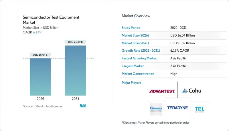
2025年半導體測試設備市值為151.1億美元,預計到2031年將達到215.9億美元,高於2026年的160.4億美元。
預計在預測期(2026-2031 年)內,複合年成長率將達到 6.13%。
需求加速成長反映了人工智慧處理器日益複雜、汽車電氣化以及新型封裝結構興起,這些都需要更精確的檢驗。隨著製造商追求更快的故障隔離和更高的整體設備效率,系統級測試、光學檢測和自適應分析的快速發展正在重塑資本配置。亞太地區貢獻了全球一半的收入,而北美和歐洲正在主權計畫的支持下擴大產能,從而推動了區域內對高階測試儀的需求。競爭優勢正向那些能夠整合探針卡、分析軟體和特定應用專業知識的供應商轉移。同時,由於資本密集度的成長速度超過了平均售價的成長速度,因此利潤率持續承壓。 ATE(自動測試設備)主要企業與探針卡專家之間的策略聯盟強調垂直整合,以此作為對沖關鍵機械介面供應鏈脆弱性的一種手段。
全球半導體測試設備市場趨勢與洞察
人工智慧/機器學習和邊緣運算對積體電路的需求不斷成長
生成式人工智慧的爆炸性成長帶來了前所未有的檢驗複雜性,並推動了對能夠測試超高引腳數元件的自動化測試儀的需求。晶圓級老化測試和系統級測試套件的訂單趨勢反映出半導體測試設備市場正轉向在加速熱應力條件下進行可靠性篩檢。人工智慧加速器整合了大晶粒面積和先進的記憶體堆疊,促使客戶投資於配備「按設計測試」功能的自適應測試儀。在人工智慧裝置需求的推動下,愛德萬測試在2024會計年度上半年實現了創紀錄的銷售額和利潤,這證實了高級檢驗已成為供應商的利潤來源,而非半導體製造商的成本中心。半導體測試設備產業正在透過整合機器學習演算法來應對這項挑戰,這些演算法可以在不影響覆蓋率的情況下縮短測試停留時間。在中期內,雲端服務供應商和超大規模資料中心營運商仍將是超高吞吐量系統級測試儀的主要買家。
汽車產業正迅速向ADAS和電動車平台轉型。
集中式車輛運算架構將資訊娛樂、電池管理和雷達處理功能整合到融合晶片上,這些晶片的功能安全必須符合 ISO 26262 標準。這一轉變擴展了測試程序的範圍,從參數檢查擴展到模擬道路事件的全面場景檢驗。是德科技的認證工具鏈支援從設計到生產的可追溯性,展現了合規標準如何影響半導體測試設備的採購。汽車級積體電路的可靠性篩檢時間幾乎是消費性電子產品的兩倍,這推動了對老化測試爐和高效節能處理器的訂單。
資本投資強度增加和平均售價下降
半導體測試設備產業面臨許多挑戰,成本上升和價格下跌影響了盈利,並限制了對新技術的投資。根據SEMI的報告,2024年全球半導體設備營收將達到1,130億美元,但隨著設備複雜性的增加,利潤率持續下降,定價權受到削弱。先進的封裝和晶片結構需要高成本的專用測試設備,而客戶為了保護利潤,這些設備面臨價格壓力。 KLA公司報告稱,由於半導體和晶圓製造設備市場環境疲軟,其2024會計年度收入下降了7%,至98億美元,凸顯了價格壓力的影響。大批量應用也帶來了額外的挑戰,因為客戶在要求先進測試功能的同時,也要降低成本。製造商正致力於自動化、標準化以及研發,以保持其技術優勢。
細分市場分析
2025年,自動化測試設備在半導體測試設備市場中維持了37.56%的佔有率,鞏固了該品類在大批量生產領域的強勁地位。該領域涵蓋SoC、記憶體和射頻測試儀,這些測試儀目前整合了人工智慧診斷功能,可加快測試覆蓋率。愛德萬測試的T5801能夠檢驗GDDR7和DDR6裝置,展現了傳統測試儀為滿足下一代記憶體頻寬需求而進行的革新。在平行測試過程中,夾具和探針設備可確保熱均勻性和精確對準,有助於降低高引腳數元件的單一測試成本。
由於晶片和3D封裝引入了傳統電學檢測無法發現的視覺缺陷,光學檢測系統預計將在半導體測試設備市場中實現最高的複合年成長率(CAGR),達到7.84%。紅外線成像、亞表面裂紋檢測和人工智慧輔助缺陷分類技術正在變革品管工作流程。隨著晶圓廠在前端和後端製程中不斷應用光學解決方案,半導體測試設備市場中光學解決方案的市場規模預計將持續擴大。電學數據和光學數據的結合能夠實現預測分析,從而降低返工率並提高一次產量比率。
區域分析
預計到2025年,亞太地區將佔據半導體測試設備市場49.62%的佔有率,並在2031年之前以7.58%的複合年成長率持續成長。台灣正在加速資本投資,金元電子投資370億新台幣(約12.4億美元)用於提升其人工智慧晶片測試能力,鞏固了其區域主導地位。中國正深化國內工具研發以因應出口限制,而東南亞國家馬來西亞和新加坡則在加強其後端技術實力,並鞏固其在矽光電的市場地位。
在北美,《晶片法案》(CHIPS Act)的激勵措施已為新晶圓廠注入超過520億美元的資金,並帶動了對測試和計量設備的同步投資。英特爾接受ASML的高數值孔徑極紫外光刻機(EUV),標誌著其在3奈米以下製程節點上的量產能力正在提升,並將加速先進自動測試設備(ATE)的普及。歐洲正透過在德勒斯登投資100億歐元(約116.5億美元)的晶圓代工廠合資企業,追求自主化發展,從而推動了汽車客戶對客製化探針卡和系統級機架的增量需求。在德國,包括英特爾和Wolfspeed在內的更廣泛的建設計畫叢集正在推動該地區工具消費的進一步多元化。
中東和非洲地區雖然仍處於發展初期,但已展現出在政策主導對半導體自給自足的濃厚興趣。波灣合作理事會(GCC)成員國正在資助設計中心和人才培養項目,這些項目有望發展成為區域性測試中心。出口管制緊張局勢擾亂了全球供應,促使各地區在國內尋求關鍵介面組件的供應。因此,半導體測試設備市場正在適應多極化的市場格局,在這個格局下,供應鏈的韌性比單純的成本最佳化更為重要。
其他福利:
- Excel格式的市場預測(ME)表
- 3個月的分析師支持
目錄
第1章 引言
- 研究假設和市場定義
- 調查範圍
第2章調查方法
第3章執行摘要
第4章 市場情勢
- 市場概覽
- 市場促進因素
- 人工智慧/機器學習和邊緣運算積體電路供應量不斷增加
- 汽車產業向ADAS和EV平台快速轉型
- 擴大3D積體電路和先進封裝的產能
- 向5奈米以下製程節點的主流過渡
- 基於晶片組的異質整合技術的興起
- 利用在線連續自適應測試分析降低OEE損失
- 市場限制
- 資本支出強度增加和平均售價下降
- 探針卡和MEMS插座的供應鏈漏洞
- 射頻測試演算法開發人才短缺
- 永續性合規成本不斷增加
- 產業價值鏈分析
- 監管環境
- 技術展望
- 宏觀經濟因素如何影響市場
- 波特五力分析
- 新進入者的威脅
- 買方的議價能力
- 供應商的議價能力
- 替代品的威脅
- 競爭對手之間的競爭
第5章 市場規模與成長預測
- 依產品類型
- 自動測試設備(ATE)
- SoC測試儀(系統晶片)
- 記憶體測試器
- 射頻測試儀
- 類比/混合訊號測試儀
- 其他自動測試設備
- 老化系統
- 搬運設備
- 探針裝置
- 光學檢測系統
- 其他設備類別
- 自動測試設備(ATE)
- 透過使用
- 晶圓分選/探測
- 期末測試
- 系統級測試
- 可靠性/老化
- 按最終用途行業分類
- 家用電子電器
- 汽車與出行
- 工業和電力
- 電訊和網路
- 醫學與生命科學
- 其他終端用戶產業
- 按地區
- 北美洲
- 美國
- 加拿大
- 墨西哥
- 南美洲
- 巴西
- 阿根廷
- 其他南美洲
- 歐洲
- 德國
- 英國
- 法國
- 俄羅斯
- 其他歐洲地區
- 亞太地區
- 中國
- 日本
- 印度
- 韓國
- 東南亞
- 亞太其他地區
- 中東和非洲
- 中東
- 沙烏地阿拉伯
- 阿拉伯聯合大公國
- 其他中東地區
- 非洲
- 南非
- 埃及
- 其他非洲地區
- 中東
- 北美洲
第6章 競爭情勢
- 市場集中度
- 策略趨勢
- 市佔率分析
- 公司簡介
- Advantest Corporation
- Teradyne Inc.
- Cohu Inc.
- Chroma ATE Inc.
- Tokyo Electron Ltd.
- Tokyo Seimitsu Co. Ltd.(Accretech)
- National Instruments Corporation
- Astronics Corporation
- TESEC Corporation
- Hon Technology Co. Ltd.
- SPEA SpA
- FormFactor Inc.
- MPI Corporation
- TSE Co. Ltd.
- Keysight Technologies Inc.
- Rohde & Schwarz GmbH & Co KG
- Test Research Inc.(TRI)
- MicroCraft Inc.
- SHIBAURA Mechatronics Corporation
- Sinfonia Technology Co. Ltd.
- UniTest Inc.
- Shenzhen RIGOL Technologies Co. Ltd.
- ChangChuan Technology Co. Ltd.
- YIK Corp.
- Bluechips Microhouse Co. Ltd.
第7章 市場機會與未來展望
The semiconductor test equipment market was valued at USD 15.11 billion in 2025 and estimated to grow from USD 16.04 billion in 2026 to reach USD 21.59 billion by 2031, at a CAGR of 6.13% during the forecast period (2026-2031).
Demand acceleration reflects the rising complexity of AI processors, automotive electrification, and new packaging architectures that necessitate more precise validation. Rapid migration toward system-level testing, optical inspection, and adaptive analytics reshapes capital allocation as manufacturers pursue faster fault isolation and higher overall equipment effectiveness. The Asia-Pacific region anchors half of global revenue, yet North America and Europe are stepping up capacity under sovereignty programs that are widening regional demand for high-end testers. Competitive advantages shift toward suppliers that combine probe cards, analytics software, and application-specific expertise, while margin pressure persists because capital intensity grows faster than average selling prices. Strategic partnerships between ATE leaders and probe card specialists emphasize vertical integration as a hedge against supply chain fragility in critical mechanical interfaces.
Global Semiconductor Test Equipment Market Trends and Insights
Increasing AI/ML and Edge-Computing IC Volumes
Explosive uptake of generative AI creates unprecedented validation complexity that elevates automated testers equipped for very-high-pin-count devices. Order momentum for wafer-level burn-in and system-level suites reflects the semiconductor test equipment market pivot toward reliability screening under accelerated thermal stress profiles. AI accelerators integrate massive die areas and advanced memory stacks, prompting customers to invest in adaptive testers that synchronize with design-for-test hooks. Advantest reported new highs for revenue and profit in the first half of fiscal 2024 based on AI device demand, confirming that verification intensity is now a profit driver for suppliers rather than a cost center for chipmakers. The semiconductor test equipment industry responds by embedding machine-learning algorithms that cut dwell time without compromising coverage. Over the medium term, cloud service providers and hyperscale data-center operators will remain the dominant purchasers of ultra-high-throughput system-level testers.
Rapid Automotive Shift Toward ADAS and EV Platforms
Centralized vehicle compute architectures merge infotainment, battery management, and radar processing onto fusion chips whose functional safety must meet ISO 26262 requirements. This transition enlarges the test program scope from parametric checks to holistic scenario validation that mirrors on-road events. Keysight's certified toolchain underpins traceability from design to production, signaling how compliance criteria shape procurement in the semiconductor test equipment market. Reliability screening time for automotive-grade ICs stands nearly 2 times consumer-grade devices, fueling orders for burn-in ovens and power-aware handlers.
Increasing CAPEX Intensity Versus ASP Erosion
The semiconductor test equipment industry faces challenges as rising costs and declining prices impact profitability and limit investments in new technologies. SEMI reported global semiconductor equipment sales reached USD 113 billion in 2024, but margin compression persists as equipment complexity outpaces pricing power. Advanced packaging and chiplet architectures require specialized testing equipment, which comes at a higher cost, and face pricing pressure from customers as they protect their margins. KLA Corporation reported a 7% decline in revenue to USD 9.8 billion in fiscal 2024, driven by weaker market conditions in the semiconductor and wafer fabrication equipment sectors, highlighting the impact of pricing pressures. High-volume applications face added challenges as customers demand cost reductions alongside advanced testing capabilities. Manufacturers are focusing on automation, standardization, and research and development to maintain technological leadership.
Other drivers and restraints analyzed in the detailed report include:
- Expansion of 3D-IC and Advanced Packaging Capacity
- Mainstream Migration to Sub-5 nm Nodes
- Supply-Chain Fragility in Probe Cards and MEMS Sockets
For complete list of drivers and restraints, kindly check the Table Of Contents.
Segment Analysis
Automated test equipment retained 37.56% of the semiconductor test equipment market share in 2025, underscoring the category's entrenched position in volume production. The segment includes SoC, memory, and RF testers that now integrate AI-enabled diagnostics to accelerate pattern coverage. Advantest's T5801 validates GDDR7 and DDR6 devices, demonstrating that conventional testers are evolving to address the next-generation memory bandwidth requirements. Handler and probe equipment ensure thermal uniformity and precise alignment during parallel testing, lowering cost-per-site for high-pin-count devices.
Optical inspection systems are projected to record an 7.84% CAGR, the fastest within the semiconductor test equipment market, as chiplet and 3D packages introduce visual defects that traditional electrical checks miss. Infrared imaging, subsurface crack detection, and AI-assisted defect classification reshape quality control workflows. The semiconductor test equipment market size associated with optical solutions is expected to increase as fabs deploy them in both front-end and back-end lines. Partnerships between electrical and optical data will enable predictive analytics that cut rework rates and uplift first-pass yield.
The Semiconductor Test Equipment Market Report is Segmented by Product Type (Automated Test Equipment, Burn-In Systems, and More), Application (Wafer Sort/Probe, Final Test, System-Level Test, Reliability/Burn-in), End-Use Industry (Consumer Electronics, Automotive and Mobility, and More), and Geography (North America, South America, Europe, Asia-Pacific, and More). The Market Forecasts are Provided in Terms of Value (USD).
Geography Analysis
Asia-Pacific dominated the semiconductor test equipment market with a 49.62% share in 2025 and is on track for a 7.58% CAGR to 2031. Taiwan accelerates capex, with King Yuan Electronics allocating NTD 37 billion (USD 1.24 billion) to boost AI chip testing capacity, underscoring regional leadership. China deepens domestic tool development to offset export controls, while Southeast Asia's Malaysia and Singapore reinforce back-end specialization and silicon-photonics niches.
North America benefits from CHIPS Act incentives that funnel over USD 52 billion into new fabs, instigating parallel investment in testers and metrology. Intel's receipt of ASML's high-NA EUV tool signals volume ramp at sub-3 nm nodes, a catalyst for advanced ATE adoption. Europe pursues sovereignty through the EUR 10 billion (USD 11.65 billion) Dresden foundry joint venture, creating incremental demand for probe cards and system-level racks tailored to automotive clients. Germany's broader cluster, including planned Intel and Wolfspeed facilities, further diversifies regional tool consumption.
The Middle East and Africa remain nascent but show policy-driven interest in semiconductor self-sufficiency. Gulf Cooperation Council states finance design centers and talent pipelines that may evolve into localized testing hubs. Export-control tensions fragment global supply, pushing regions to secure critical interface components internally. The semiconductor test equipment market, therefore, adapts to a multipolar landscape in which supply-chain resiliency trumps pure cost optimization.
- Advantest Corporation
- Teradyne Inc.
- Cohu Inc.
- Chroma ATE Inc.
- Tokyo Electron Ltd.
- Tokyo Seimitsu Co. Ltd. (Accretech)
- National Instruments Corporation
- Astronics Corporation
- TESEC Corporation
- Hon Technology Co. Ltd.
- SPEA S.p.A.
- FormFactor Inc.
- MPI Corporation
- TSE Co. Ltd.
- Keysight Technologies Inc.
- Rohde & Schwarz GmbH & Co KG
- Test Research Inc. (TRI)
- MicroCraft Inc.
- SHIBAURA Mechatronics Corporation
- Sinfonia Technology Co. Ltd.
- UniTest Inc.
- Shenzhen RIGOL Technologies Co. Ltd.
- ChangChuan Technology Co. Ltd.
- YIK Corp.
- Bluechips Microhouse Co. Ltd.
Additional Benefits:
- The market estimate (ME) sheet in Excel format
- 3 months of analyst support
TABLE OF CONTENTS
1 INTRODUCTION
- 1.1 Study Assumptions and Market Definition
- 1.2 Scope of the Study
2 RESEARCH METHODOLOGY
3 EXECUTIVE SUMMARY
4 MARKET LANDSCAPE
- 4.1 Market Overview
- 4.2 Market Drivers
- 4.2.1 Increasing AI/ML and edge-computing IC volumes
- 4.2.2 Rapid automotive shift toward ADAS and EV platforms
- 4.2.3 Expansion of 3 D-IC and advanced packaging capacity
- 4.2.4 Mainstream migration to sub-5 nm nodes
- 4.2.5 Emergence of chiplet-based heterogeneous integration
- 4.2.6 In-line adaptive test analytics reducing OEE losses
- 4.3 Market Restraints
- 4.3.1 Increasing CAPEX intensity vs ASP erosion
- 4.3.2 Supply-chain fragility in probe cards and MEMS sockets
- 4.3.3 Talent crunch in RF test algorithm development
- 4.3.4 Escalating sustainability compliance costs
- 4.4 Industry Value Chain Analysis
- 4.5 Regulatory Landscape
- 4.6 Technological Outlook
- 4.7 Impact of Macroeconomic Factors on the Market
- 4.8 Porter's Five Forces Analysis
- 4.8.1 Threat of New Entrants
- 4.8.2 Bargaining Power of Buyers
- 4.8.3 Bargaining Power of Suppliers
- 4.8.4 Threat of Substitute Products
- 4.8.5 Intensity of Competitive Rivalry
5 MARKET SIZE AND GROWTH FORECASTS (VALUE)
- 5.1 By Product Type
- 5.1.1 Automated Test Equipment (ATE)
- 5.1.1.1 SoC Testers (System-on-Chip)
- 5.1.1.2 Memory Testers
- 5.1.1.3 RF Testers
- 5.1.1.4 Analog/Mixed-Signal Testers
- 5.1.1.5 Other Automated Test Equipments
- 5.1.2 Burn-in Systems
- 5.1.3 Handler Equipment
- 5.1.4 Probe Equipment
- 5.1.5 Optical Inspection Systems
- 5.1.6 Other Equipment Categories
- 5.1.1 Automated Test Equipment (ATE)
- 5.2 By Application
- 5.2.1 Wafer Sort / Probe
- 5.2.2 Final Test
- 5.2.3 System-Level Test
- 5.2.4 Reliability / Burn-in
- 5.3 By End-use Industry
- 5.3.1 Consumer Electronics
- 5.3.2 Automotive and Mobility
- 5.3.3 Industrial and Power
- 5.3.4 Telecommunications and Networking
- 5.3.5 Healthcare and Life-science
- 5.3.6 Other End-use Industries
- 5.4 By Geography
- 5.4.1 North America
- 5.4.1.1 United States
- 5.4.1.2 Canada
- 5.4.1.3 Mexico
- 5.4.2 South America
- 5.4.2.1 Brazil
- 5.4.2.2 Argentina
- 5.4.2.3 Rest of South America
- 5.4.3 Europe
- 5.4.3.1 Germany
- 5.4.3.2 United Kingdom
- 5.4.3.3 France
- 5.4.3.4 Russia
- 5.4.3.5 Rest of Europe
- 5.4.4 Asia-Pacific
- 5.4.4.1 China
- 5.4.4.2 Japan
- 5.4.4.3 India
- 5.4.4.4 South Korea
- 5.4.4.5 South-East Asia
- 5.4.4.6 Rest of Asia-Pacific
- 5.4.5 Middle East and Africa
- 5.4.5.1 Middle East
- 5.4.5.1.1 Saudi Arabia
- 5.4.5.1.2 United Arab Emirates
- 5.4.5.1.3 Rest of Middle East
- 5.4.5.2 Africa
- 5.4.5.2.1 South Africa
- 5.4.5.2.2 Egypt
- 5.4.5.2.3 Rest of Africa
- 5.4.5.1 Middle East
- 5.4.1 North America
6 COMPETITIVE LANDSCAPE
- 6.1 Market Concentration
- 6.2 Strategic Moves
- 6.3 Market Share Analysis
- 6.4 Company Profiles (includes Global level Overview, Market level overview, Core Segments, Financials as available, Strategic Information, Market Rank/Share for key companies, Products and Services, and Recent Developments)
- 6.4.1 Advantest Corporation
- 6.4.2 Teradyne Inc.
- 6.4.3 Cohu Inc.
- 6.4.4 Chroma ATE Inc.
- 6.4.5 Tokyo Electron Ltd.
- 6.4.6 Tokyo Seimitsu Co. Ltd. (Accretech)
- 6.4.7 National Instruments Corporation
- 6.4.8 Astronics Corporation
- 6.4.9 TESEC Corporation
- 6.4.10 Hon Technology Co. Ltd.
- 6.4.11 SPEA S.p.A.
- 6.4.12 FormFactor Inc.
- 6.4.13 MPI Corporation
- 6.4.14 TSE Co. Ltd.
- 6.4.15 Keysight Technologies Inc.
- 6.4.16 Rohde & Schwarz GmbH & Co KG
- 6.4.17 Test Research Inc. (TRI)
- 6.4.18 MicroCraft Inc.
- 6.4.19 SHIBAURA Mechatronics Corporation
- 6.4.20 Sinfonia Technology Co. Ltd.
- 6.4.21 UniTest Inc.
- 6.4.22 Shenzhen RIGOL Technologies Co. Ltd.
- 6.4.23 ChangChuan Technology Co. Ltd.
- 6.4.24 YIK Corp.
- 6.4.25 Bluechips Microhouse Co. Ltd.
7 MARKET OPPORTUNITIES AND FUTURE OUTLOOK
- 7.1 White-space and Unmet-need Assessment
 CoC老化測試儀市場按技術、腔室類型、壓力範圍、應用和最終用途分類,全球預測(2026-2032年)
 2026年全球印刷基板檢測設備市場報告2026年半導體檢測透鏡全球市場報告
 全球半導體測試設備市場:市場規模、佔有率、成長率、產業分析、依類型、應用和地區劃分的分析以及未來預測(2026-2034)SoC 和記憶體半導體測試儀市場(按測試模式、測試儀類型、製程節點、封裝類型、應用和最終用戶分類)—2026-2032 年全球預測SoC老化測試設備市場按容量、技術節點、處理器類型、測試解決方案和應用分類 - 全球預測(2026-2032年)半導體自動管理儲存系統 (AMHS) 市場按系統類型、晶圓尺寸、自動化程度、連接埠類型、應用和最終用戶分類 - 全球預測 2026-2032 年探針台系統市場按類型、晶圓尺寸、技術、晶圓材料、應用和最終用戶分類 - 全球預測 2026-2032晶片測試用矽橡膠插座市場:按插座類型、觸點材質、間距、引腳數、應用和最終用戶分類 - 全球預測 2026-2032
 全球半導體測試設備市場展望、詳細分析及至2031年預測