


 |
市場調查報告書
商品編碼
1644780
3D IC封裝:市場佔有率分析、產業趨勢與統計、成長預測(2025-2030 年)3D IC Packaging - Market Share Analysis, Industry Trends & Statistics, Growth Forecasts (2025 - 2030) |
||||||
價格
※ 本網頁內容可能與最新版本有所差異。詳細情況請與我們聯繫。
簡介目錄
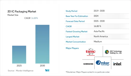
預測期內 3D IC封裝市場預計複合年成長率為 16.8%
關鍵亮點
- 在不斷發展的微電子和半導體產業中,垂直堆疊積體電路(IC)的趨勢正在不斷發展,並成為一種可行的解決方案,可提供高性能、功能性和低功耗,以滿足電子設備的要求。連網型設備、平板電腦、智慧型手機和其他電子產品正在推動對先進架構的快速需求,以提高能源效率、效能,並且不僅僅是發送簡訊和通話。這些因素預計將推動 3D IC封裝市場的成長。
- 由於半導體應用的不斷增加,CMOS 擴展放緩和成本上升迫使產業轉向先進的 IC 封裝。 3D增材技術已成為滿足機器學習、人工智慧和資料中心等應用效能要求的有利解決方案。因此,在預測期內,對高效能運算應用的不斷成長的需求將推動 3D-TSV(矽通孔)市場的發展。
- 此外,電子設備的持續小型化也有望成為市場成長的驅動力。平板電腦、智慧型手機和遊戲設備對先進架構的需求不斷成長,以及感測器和 MEMS 中先進晶圓層次電子構裝技術的使用激增,預計將在預測期內為 3D IC封裝市場提供成長前景。根據WSTS預測,2021年半導體IC市場收益可望達4,630億美元,2022年將成長10%以上,達到5,109.6億美元。
- 新冠肺炎疫情為各行各業帶來重大影響,同時也促進了全球先進醫療設備及器材的發展。各醫療設備製造公司宣布,疫情爆發後,將增加多種新儀器設備的產量。由於 3D IC封裝在醫療產業的應用非常廣泛,預計製造業舉措的增加將推動對 3D IC封裝的需求。
- 然而,高昂的初始投資和半導體積體電路設計的日益複雜性預計會抑制市場的發展。
3D IC封裝市場趨勢
資訊科技和通訊產業可望強勁成長
- 3D IC封裝是半導體製造和設計中的重要元素。從宏觀層面來看,它影響性能、功率和成本;從微觀層面來看,它直接影響每個晶片的基本功能。
- 5G 基礎設施投資不斷增加、資料中心和伺服器數量不斷增加,再加上物聯網連接和網路設備,這些都是推動 IT 和通訊領域 3D IC封裝成長的因素。例如,包括 KT、LG Uplus 和 SK Telecom 在內的韓國行動電話營運商已同意在 2022 年投資總計 25.7 兆韓元,以支援全國的 5G 基礎設施。追加投資將集中用於提升首爾等六個城市的5G品質。
- 資料中心的擴張為研究3D IC封裝的供應商提供了成長機會。根據思科公司預測,2021年全球資料中心儲存的巨量資料量將達到Exabyte,其中美國佔了很大比例。到 2021 年,超大規模資料中心的數量將從 2015 年的 259 個增加到 700 個。
- 此外,物聯網市場的發展和無線技術需求的激增(更小的佔用空間和更高的效率是關鍵)預計將推動 3D IC封裝市場的發展。根據愛立信預測,到 2027 年,廣域物聯網設備數量將從 2021 年的 21 億增加到 52 億。
預計亞太地區將出現顯著成長
- 亞太地區是主要半導體晶片製造商和公司的所在地,例如台積電、中芯國際、聯電和韓國三星。一家領先的台灣晶片代工廠正在與日本供應商合作,爭奪關鍵的 3 奈米晶片市場的主導地位。例如,2021年2月,台積電宣布將在日本科學城筑波建立研發中心,與日本供應商合作開發3D IC封裝材料。
- 另外,2021年5月,日本經濟產業省及其下屬機構日本產業技術綜合研究所宣布,約20家日本公司將與台積電日本3D IC研發中心合作。
- 亞太地區也佔據了 3D IC封裝市場的很大佔有率,因為該地區擁有大量半導體製造業務,並且擁有三星電子、東芝公司、日月光集團和聯華電子等主要市場參與企業。
- 亞太地區以其強大的汽車製造能力而聞名。此外,5G技術在汽車產業的不斷商業化,為受調查市場中的供應商帶來了新的收益來源。基於 5G NR 的 C-V2X 的出現有望為自動駕駛汽車提供獨特的功能。這可能推動對更高水準的自主性和可預測性以及車輛內其他 ADAS 感測器技術的需求。
- 此外,該地區的市場參與企業正專注於下一代晶片技術,這可以透過 3D 封裝工具開啟新的可能性。例如,日本工具製造商 Disco 專注於 3D 晶片封裝,其中涉及在薄的、幾乎透明的矽晶片上堆疊積體電路。隨著莫耳定律接近其物理極限,晶片製造商正在探索新的設計和材料來提高下一代硬體的性能。預計這些趨勢將推動該地區的成長。
- 在目前的智慧型設備和互聯世界環境下,客戶要求下一代設備更緊湊、功能更多、性能更佳、功耗更低。這使得對於具成本效益、高性能 IC 的需求日益增加。例如,STAR 的微電子實驗室與領先的半導體公司合作開發具有成本效益的 3D 晶圓級積體電路封裝解決方案。該公司已推出晶圓晶片聯盟 II 和成本效益內插器聯盟,以推進大批量生產的晶片封裝解決方案。這個以產業為重點的聯盟致力於解決晶圓層次電子構裝中的關鍵挑戰,以降低整體製造成本並加快下一代電子設備的上市時間。
3D IC封裝產業概況
全球 3D IC封裝市場因 Amkor Technology Inc.、ASE Group 和 Siliconware Precision Industries (SPIL) 等主要參與者的存在而呈現細分化。市場參與企業必須不斷創新,提供先進、全面的產品。
- 2021 年 5 月:英特爾計劃投資 35 億美元升級其裡奧蘭喬工廠,將這個龐大的綜合體(美國三大製造地之一)的員工數量增加 35% 以上。英特爾正在擴建其新墨西哥工廠,以利用其 Foberos 3D 封裝技術生產新一代晶片。
其他福利
- Excel 格式的市場預測 (ME) 表
- 3 個月的分析師支持
目錄
第 1 章 簡介
- 研究假設和市場定義
- 研究範圍
第2章調查方法
第3章執行摘要
第4章 市場洞察
- 市場概況
- 產業吸引力-波特五力分析
- 新進入者的威脅
- 購買者/消費者的議價能力
- 供應商的議價能力
- 替代品的威脅
- 競爭對手之間的競爭強度
- 價值鏈分析
- COVID-19 市場影響評估
第5章 市場動態
- 市場促進因素
- 電子產品先進架構
- 電子設備小型化
- 市場問題/顧慮
- 半導體IC設計初期投入高,複雜度增加
第6章 市場細分
- 封裝技術
- 3D 晶圓級晶片規模封裝
- 3D TSV
- 最終用戶產業
- 家用電子電器
- 航太和國防
- 醫療設備
- 通訊和電訊
- 車
- 其他
- 地區
- 北美洲
- 歐洲
- 亞太地區
- 拉丁美洲
- 中東和非洲
第7章 競爭格局
- 公司簡介
- Taiwan Semiconductor Manufacturing Company Limited
- Samsung Electronics Co., Ltd.
- ASE Group
- Amkor Technology
- Intel Corporation
- Siliconware Precision Industries Co. Ltd(SPIL)
- GlobalFoundries
- Invensas
- Powertech Technology Inc.
第8章投資分析
第9章:市場的未來
簡介目錄
Product Code: 91074
The 3D IC Packaging Market is expected to register a CAGR of 16.8% during the forecast period.
Key Highlights
- The growing microelectronics and semiconductor industry is developing a trend for vertically stacked integrated circuits (ICs), emerging as a viable solution for providing high performance, increased functionality, and reducing power consumption to fulfill electronic device requirements. The surging need for advanced architecture in electronic products such as connected devices, tablets, and smartphones to increase their energy efficiency and performance to do more than just texting and calling. Such factors are expected to bolster the growth of the 3D IC packaging market.
- As a result of the growing semiconductor applications, the slowdown in CMOS scaling and escalating costs have forced the industry to depend on packaging advancements for ICs. 3D stacking technologies have emerged as lucrative solutions that meet the required performance of applications such as machine learning, AI, and data centers. Therefore, the growing need for high-performance computing applications drives the 3D-TSV (Through Silicon Via) market over the forecast period.
- The increasing miniaturization of electronics devices is also anticipated to drive market growth. Growing demand for advanced architecture in tablets, smartphones, and gaming devices, along with surging usage of advanced wafer-level packaging technologies in sensors and MEMS, is expected to provide growth prospects for the 3D IC packaging market during the forecast period. According to WSTS, the IC market for semiconductors reached USD 463 billion in revenue in 2021 and is expected to grow by over 10% to USD 510.96 billion in 2022.
- The COVID-19 pandemic has significantly impacted various industries and has simultaneously propelled the development of advanced medical equipment and devices across the globe. Various medical equipment manufacturing companies announced to increase in the production of several new equipment and devices post the pandemic outbreak. As the applications of 3D IC packaging are numerous within the medical and healthcare industry, the increased manufacturing initiatives are expected to boost the demand for 3D IC packaging.
- However, the high Initial Investment and Increasing Complexity of Semiconductor IC Designs are expected to restrain the evolution of the market.
3D IC Packaging Market Trends
IT & Telecommunication is Expected to Witness Significant Growth
- 3D IC Packaging is an essential part of semiconductor manufacturing and design. It directly affects performance, power, and cost on a macro level and the basic functionality of all chips on a micro level.
- The increasing investment in 5G infrastructure and the growing number of data center servers coupled with IoT connections and networking devices are the factors propelling the growth of 3D IC packaging in the IT and telecommunication sector. For instance, mobile operators in Korea such as KT, LG Uplus, and SK Telecom agreed to invest a total of KRW 25.7 trillion through 2022 to support 5G infrastructure across the country. The additional investment is focused on enhancing the 5G quality in Seoul and six other cities.
- The expansion of data centers provides a growth opportunity for the vendors in the 3D IC packaging studied. According to Cisco Systems, the amount of big data in data center storage global is anticipated to reach 403 exabytes in 2021, with a significant share in the US. Hyperscale data centers reached 700 in 2021, compared to 259 in 2015.
- Moreover, the growing IoT market and surging demand for wireless technologies, wherein reduced footprint and enhanced efficiency are critical, are expected to develop the market for 3D IC packaging. According to Ericson, wide-area IoT devices will reach 5.2 billion by 2027 from 2.1 billion in 2021.
Asia-Pacific is Expected to Witness Significant Growth Rate
- Asia Pacific is home to some of the biggest semiconductor chip manufacturers and companies like TSMC, SMIC, UMC, and South Korea's Samsung. Taiwan's leading chip foundry is teaming up with Japanese suppliers in the race to lead the crucial 3-nanometer chip market. For instance, in February 2021, TSMC announced that the company plans to establish an R&D center in Japan's science city of Tsukuba to develop 3D IC packaging materials in cooperation with its Japanese suppliers.
- Also, in May 2021, Japan's Ministry of Economy, Trade, and Industry and its subsidiary, the National Institute of Advanced Industrial Science and Technology, announced that approximately 20 Japanese companies would work with TSMC Japan's 3D IC R&D Center.
- The Asia Pacific region also holds a significant share in the 3D IC packaging market due to a considerable number of semiconductor manufacturing operations happening in the region, along with the presence of major market players such as Samsung Electronics Co., Ltd., Toshiba Corp, ASE Group, and United Microelectronics Corp. among others.
- The Asia Pacific region is known for its robust Automotive manufacturing capabilities. Moreover, the growing commercialization of 5G technology in the automotive industry will provide a new revenue stream for the vendors operating in the studied market. The advent of 5G NR-based C-V2X is anticipated to offer unique capabilities for the autonomous vehicle. Thus, it can propel the need for higher levels of autonomy and predictability and other ADAS sensor technologies in the vehicle.
- Additionally, market players in the region are forcing on Next-gen chip technology, which could unlock new potential with 3D packaging tools. For instance, Japanese tool-making company Disco focuses on 3D chip packaging by stacking integrated circuits on silicon wafers of near-transparent thinness. As Moore's Law nears its physical limits, chipmakers seek new designs and materials to get better performance out of next-generation hardware. Such trends are expected to propel growth in the region.
- In the current scenario of smart devices and the connected world, customers demand next-generation devices that are more compact, multi-functional, offer better performance, and consume less power. This has propelled the demand for cost-efficient and high-performance IC. For instance, STAR's Institute of Microelectronics has partnered with leading semiconductor companies to develop cost-effective 3D wafer-level integrated circuit packaging solutions. The company has launched chip-on-wafer consortium II and the cost-effective Interposer consortium to advance chip packaging solutions for high-volume manufacturing. The industry-focused consortium will address key challenges in wafer-level packaging to low overall manufacturing costs to accelerate time-to-market for next-generation electronics devices.
3D IC Packaging Industry Overview
The Global 3D IC Packaging Market is fragmented due to the presence of significant players such as Amkor Technology Inc., ASE Group, and Siliconware Precision Industries Co. Ltd (SPIL), among others. The market players must constantly innovate advanced and comprehensive products to stay relevant.
- In May 2021: Intel plans to invest USD 3.5 billion to upgrade its Rio Rancho plant and increase its headcount by more than 35% at the sprawling complex, one of its three largest US manufacturing hubs. It is expanding its New Mexico operations to manufacture new generations of chips based on its Foveros 3D packaging technology, which could aid the company's attempts to regain its leadership status in the semiconductor industry.
Additional Benefits:
- The market estimate (ME) sheet in Excel format
- 3 months of analyst support
TABLE OF CONTENTS
1 INTRODUCTION
- 1.1 Study Assumptions and Market Definition
- 1.2 Scope of the Study
2 RESEARCH METHODOLOGY
3 EXECUTIVE SUMMARY
4 MARKET INSIGHT
- 4.1 Market Overview
- 4.2 Industry Attractiveness - Porter's Five Forces Analysis
- 4.2.1 Threat of New Entrants
- 4.2.2 Bargaining Power of Buyers/Consumers
- 4.2.3 Bargaining Power of Suppliers
- 4.2.4 Threat of Substitute Products
- 4.2.5 Intensity of Competitive Rivalry
- 4.3 Value Chain Analysis
- 4.4 Assessment of the Impact of COVID-19 on the Market
5 MARKET DYNAMICS
- 5.1 Market Drivers
- 5.1.1 Growing Advanced Architecture in Electronic Products
- 5.1.2 Miniaturization of Electronics Devices
- 5.2 Market Challenges/Restrains
- 5.2.1 High Initial Investment and Increasing Complexity of Semiconductor IC Designs
6 MARKET SEGMENTATION
- 6.1 Packaging Technology
- 6.1.1 3D wafer-level chip-scale packaging
- 6.1.2 3D TSV
- 6.2 End-User Industry
- 6.2.1 Consumer electronics
- 6.2.2 Aerospace and Defense
- 6.2.3 Medical Devices
- 6.2.4 Communications and Telecom
- 6.2.5 Automotive
- 6.2.6 Others
- 6.3 Geography
- 6.3.1 North America
- 6.3.2 Europe
- 6.3.3 Asia-Pacific
- 6.3.4 Latin America
- 6.3.5 Middle-East and Africa
7 COMPETITIVE LANDSCAPE
- 7.1 Company Profiles
- 7.1.1 Taiwan Semiconductor Manufacturing Company Limited
- 7.1.2 Samsung Electronics Co., Ltd.
- 7.1.3 ASE Group
- 7.1.4 Amkor Technology
- 7.1.5 Intel Corporation
- 7.1.6 Siliconware Precision Industries Co. Ltd (SPIL)
- 7.1.7 GlobalFoundries
- 7.1.8 Invensas
- 7.1.9 Powertech Technology Inc.
8 INVESTMENT ANALYSIS
9 FUTURE OF THE MARKET
02-2729-4219
+886-2-2729-4219
 2025 年 3D IC 和 2.5D IC封裝全球市場報告
 IC封裝市場規模、佔有率、成長分析,按類型、按技術、按材料、按最終用戶、按地區 - 行業預測,2025-2032 年
 3D IC 和 2.5D IC封裝市場:按技術、最終用戶、應用分類 - 2025-2030 年全球預測先進IC封裝市場:按類型、應用分類 - 2025-2030 年全球預測電源管理IC封裝市場:按類型、解決方案和應用分類 - 2025-2030 年全球預測
 引線框架市場:市場規模及預測(2024年~2025年)
 晶片級封裝 (CSP) LED 市場、機會、成長動力、產業趨勢分析與預測,2024-2032 年
 晶片級封裝(CSP)LED 市場:2024-2033年全球產業分析、規模、佔有率、成長、趨勢、預測3D IC和2.5D IC市場:全球產業分析,規模,佔有率,成長,趨勢,預測,2024年~2032年
 晶片級封裝 (CSP) LED 市場,依功率範圍、依應用、最終用戶、國家和地區分類 - 2024-2032 年行業分析、市場規模、市場佔有率和預測
▼