 |
市場調查報告書
商品編碼
1630292
嵌入式晶片封裝-市場佔有率分析、產業趨勢與統計、成長預測(2025-2030)Embedded Die Packaging - Market Share Analysis, Industry Trends & Statistics, Growth Forecasts (2025 - 2030) |
||||||
※ 本網頁內容可能與最新版本有所差異。詳細情況請與我們聯繫。
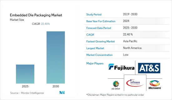
嵌入式晶片封裝市場預計在預測期間內複合年成長率為 22.4%

主要亮點
- 隨著產品變得更小、更豐富,設備小型化推動市場從生物醫學應用到化學微反應器和感測器,微機械加工和奈米技術將在組件的小型化中發揮越來越重要的作用。例如,藍牙無線 LAN 模組在當今的高密度行動裝置中需要最小的電路基板空間。
- 電氣和熱性能的改進正在推動市場發展。在電源管理和行動無線應用中,嵌入式技術因其薄型和卓越的熱性能而被視為組裝製造的替代方案。嵌入式晶粒的熱性能比銅夾的 PQFN 提高約 17%。對於電動車,我們還開發了一種用於功率元件的新型可擴展先進封裝,該封裝使用嵌入式晶粒和線路重布(RDL) 技術來提高電氣和熱性能。
- 此外,由於其在高頻下優異的電氣性能,該技術也被認為是新興 IT 和通訊應用的一項有前途的技術。有助於在通訊應用中部署該技術的各種好處包括改進電子電路的功能和效率、改進功率和訊號電感、提高可靠性以及增加訊號密度。
- 嵌入式晶粒技術難以測試、檢查和重工,是市場成長的挑戰。當特徵(線條和空間)變得小於 2μm 時,就很難看到缺陷。此外,根據應用的不同,在通孔內尋找碎片也成為一個問題。
- 自COVID-19爆發以來,電子產業受到重創,供應鏈和生產設施受到嚴重影響。 2 月至 3 月,中國大陸和台灣地區停產,影響了全球各OEM。
嵌入式晶片封裝市場趨勢
軟基板晶粒可望佔據較大市場佔有率
- 隨著技術的進步,印刷基板的產品銷售量不斷增加,隨著軟性基板擴大應用於各種穿戴式和物聯網設備,未來銷售量預計將進一步增加。
- 伸縮性電子裝置 (SC) 目前已在商業性銷售,並有多種形狀和形式。該技術主要使用稱為軟性基板的標準印刷電路基板,並使用液體射出成型技術來形成包含合成橡膠體的可拉伸電子電路,從而產生堅固可靠的產品。例如,在軍事應用中,靈活、輕巧的衝擊感測器可以嵌入製服和裝甲中,以儲存有關戰鬥中受傷的資訊並提供更好的情報。
- 軟性混合電子(FHE)被認為是電子電路製造的新方法,旨在結合傳統電子和印刷電子的優勢。 IC 採用微影術製造並作為裸晶安裝。
- 由於軟性電路在各種小型電子設備中的實現,其嵌入活動往往很高。例如,2019 年 9 月,IDEMIA 和 Zwipe 合作開發了生物識別付款卡解決方案,其中安全元件和微控制器等全部整合到安裝在軟性印刷電路基板的單一晶片中,計畫透過零件數量相對較少。
- 此外,運動應用和醫療應用的自主系統主要受益於小尺寸,因為精細的結構提供了最大的靈活性和舒適度。透過將現成的 IC 整合到軟性電路基板(FCB) 中,可以縮小整個系統的尺寸。使用液晶聚合物 (LCP) 作為感測器基板在醫療產品中非常常見。用於醫療應用的微型智慧感測器模組可以使用傳統的軟性電路薄膜和標準組裝製程和設備,由 LCP基板製造。
預計北美將佔據較大市場佔有率
- 美國也是半導體封裝創新的領導者,在 19 個州擁有 80 家晶圓廠,引進嵌入式晶粒小型化等新技術。另外,跨國公司對美國的投資正在提振市場。
- 例如,英特爾正在利用英特爾的 3D系統級封裝技術,透過嵌入式晶片互連橋 (EMIB) 來支援下一代平台。業界將這種應用稱為2.5D封裝整合。 EMIB(嵌入式多晶片互連橋)使用具有多個佈線層的非常小的橋晶片,而不是使用其他 2.5D 方法中常見的大型矽內插器。此橋晶粒是我們基板製造過程的一部分。
- 除此之外,美國還有一些世界領先的汽車製造商投資電動車領域。嵌入式系統透過主動車距控制巡航系統等駕駛輔助功能提高了駕駛舒適度。要達到顯著的節能,還需要採用分散式嵌入式控制方法來控制整個車輛的電源管理。這將增加對嵌入式晶粒技術的需求。
嵌入式晶片封裝產業概述
由於汽車、工業和家用電子電器最終用戶數量不斷增加,嵌入式晶片封裝市場變得支離破碎。市場上的現有參與企業正試圖透過適應 5G通訊、高性能資料中心和小型電子產品等新技術來保持競爭力。主要參與企業包括 Microsemi Corporation 和 Fujikura Ltd.。近期市場發展趨勢如下。
- 2020 年 10 月 -美國國防部將異質整合原型 (SHIP) 計畫第二階段授予英特爾聯邦有限責任公司。 SHIP計畫讓美國政府可以利用英特爾在亞利桑那州和奧勒岡州的尖端半導體封裝能力,利用英特爾每年數百億美元的研發和製造投資所創造的能力。該計劃將由海軍水面作戰中心起重機分部執行,並由國家安全技術加速器管理。
- 2019 年 9 月 - 基於 FPGA 的硬體加速器元件和高效能 eFPGA IP 的領先供應商 Achronix 半導體公司已加入台積電 IP 聯盟計劃,該計劃是台積電開放創新平台 (OIP) 的關鍵組成部分。在台積電開放創新平台生態系統論壇的展位上,Achronix 展示了其 Speedcore IP 如何針對每個客戶應用進行獨特的調整和最佳化。
其他好處
- Excel 格式的市場預測 (ME) 表
- 3 個月分析師支持
目錄
第1章簡介
- 研究假設和市場定義
- 調查範圍
第2章調查方法
第3章執行摘要
第4章市場動態
- 市場概況
- 市場促進因素
- 設備小型化的進展
- 改善電氣和熱性能
- 市場限制因素
- 檢查、測試和返工困難
- 價值鏈分析
- 產業吸引力-波特五力分析
- 供應商的議價能力
- 買家/消費者的議價能力
- 新進入者的威脅
- 替代品的威脅
- 競爭公司之間敵對關係的強度
- COVID-19 對市場的影響
第5章技術概況
- PCB小型化
- 先進的嵌入式主動系統整合
第6章 市場細分
- 平台
- 硬基板晶粒
- 軟體基板晶粒
- IC封裝基板
- 最終用戶
- 消費性電子產品
- 資訊科技/通訊
- 車
- 醫療保健
- 其他
- 地區
- 美洲
- 歐洲/中東/非洲
- 亞太地區
第7章 競爭格局
- 公司簡介
- Microsemi Corporation
- Fujikura Ltd
- Infineon Technologies AG
- ASE Group
- AT&S Company
- Schweizer Electronic AG
- Intel Corporation
- Taiwan Semiconductor Manufacturing Company
- Shinko Electric Industries Co. Ltd
- Amkor Technology
- TDK Corporation
第8章投資分析
第9章 市場機會及未來趨勢
The Embedded Die Packaging Market is expected to register a CAGR of 22.4% during the forecast period.

Key Highlights
- Growing miniaturization of devices is driving the market as products are becoming increasingly smaller and embed more functionality. Micromachining and nanotechnology play an increasingly important role in the miniaturization of components ranging from biomedical applications to chemical microreactors and sensors. For instance, Bluetooth wifi modules requires minimal circuit board area on today's high-density mobile devices.
- Improved electrical & thermal performance is driving the market. For power management and mobile-wireless application the embedded technology has been evaluated to replace assembles fabrication by not only thinner thickness but due to superior thermal performance. The thermal performance of embedded die is better than PQFN with copper clip about 17%. Also a new and expandable advanced package for power devices is developed using embedded dies and redistribution layer (RDL) technology for electric car to improve the electric and thermal performance.
- Further, owing to its excellent electrical performance at high frequencies, the technology is also being perceived as a promising technology for emerging telecommunication applications. Various advantages that aid the deployment of the technology in telecommunication applications include increased functionality and efficiency of the electronic circuits, power and signal inductance, improved reliability, and higher signal density.
- Difficulty to test, inspect and rework, the embedded die technology challenges the market to grow. As features (lines and spaces) shrink to 2µm and below, it becomes more difficult to see defects. In addition, finding debris in via holes becomes a concern in some applications.
- Since the outbreak of COVID-19, the electronics industry has been hit severely, with a significant influence on its supply chain and production facilities. The production came to a stand still in China and Taiwan during February and March, which influenced various OEMs across the world.
Embedded Die Packaging Market Trends
Die in Flexible Board Expected to Hold Significant Market Share
- With the increased advancement in technology, the product sale value of the printed circuit board is increasing and with the increased adoption of the flexible board in various wearable and IoT devices, the sales are expected to grow higher in future.
- Stretchable Electronics (SC) is so far commercial and comes in many shapes and forms. The technology uses standard printed circuit board, mainly flexible board, where liquid injection molding techniques involve elastomer embedded stretchable electronic circuit, which achieves a robust and reliable product. For instance, in military usage, uniforms and armors can have embedded, flexible, lightweight impact sensors that could store and provide better information of the injury sustained during combat.
- Flexible hybrid electronics (FHE), which is considered as a novel approach to electronic circuit manufacturing, aims to combine the best of conventional and printed electronics. Additional components and as many as conductive interconnects are possible to be printed onto a flexible substrate, whereas the IC is produced using photolithography and then mounted, as a bare die.
- The embedding activity of flexible circuits are in high trend for their implementation in various miniature electronic devices. For instance, in September 2019, IDEMIA and Zwipe collaborated for a biometric payment card solution, where the solution is planned to be distinguished by its relatively small number of components, with things, like the Secure Element and the microcontroller, all embedded in a single chip mounted on a flexible printed circuit board.
- Further, autonomous systems for sports applications and healthcare mainly benefit from a small form factor, as minute structures result in maximal flexibility and comfort. The embedding of a commercially available IC in a flexible circuit board (FCB) can reduce the overall size of a system. The usage of liquid crystal polymer (LCP) as base material for sensors are highly used in medical products. Miniaturized smart sensor modules for medical applications can be fabricated from LCP substrates using conventional flex circuit thin film and standard assembly processes and equipment.
North America Expected to Hold Significant Market Share
- Countries in the region, such as United States assist the world in manufacturing, designing, and researching related to the semiconductor industry and United States is also the frontrunner in semiconductor packaging innovation having 80 wafer fabrication plants spread across 19 states where new technologies is being implemented such as miniaturization through embedded die etc. Apart from this, investments in this country by global players are setting to fuel the market.
- For instance, Intel is enabling Next-Generation Platforms using Intel's 3D System-in-package technology through Embedded Multi-die Interconnect Bridge (EMIB) , an elegant and cost-effective approach to in-package high density interconnect of heterogeneous chips. The industry refers to this application as 2.5D package integration. Instead of using a large silicon interposer typically found in other 2.5D approaches, Embedded Multi-die Interconnect Bridge (EMIB) uses a very small bridge die, with multiple routing layers. This bridge die is embedded as part of our substrate fabrication process.
- Apart from this, the United States is home to some of the major automotive players in the world, which are investing in the electric car segment. The embedded systems increases the driving comfort with driver assistance functions like adaptive cruise control. Also to achieve significant energy savings, a distributed embedded control approach becomes necessary to control the power management of the entire vehicle. This is set to increase the demand for embedded die technology.
Embedded Die Packaging Industry Overview
The embedded die packaging market is fragmented due to the growing number of end-users in automotive, industrial, and consumer electronics. The existing players in the market are striving to maintain a competitive edge by catering to newer technologies, such as 5G telecommunication, high-performance data centers, compact electronic devices, etc. Key players are Microsemi Corporation, Fujikura Ltd, etc. Recent developments in the market are -
- October 2020 - The U.S. Department of Defence awarded Intel Federal LLC the second phase of its Heterogeneous Integration Prototype (SHIP) program. The SHIP program enables the US government to access Intel's state-of-the-art semiconductor packaging capabilities in Arizona and Oregon and take advantage of capabilities created by Intel's tens of billions of dollars of annual R&D and manufacturing investment. The project is executed by the Naval Surface Warfare Centre, Crane Division, and administered by the National Security Technology Accelerator.
- Sep 2019 - Achronix Semiconductor Corporation, a leading supplier in FPGA-based hardware accelerator devices and high-performance eFPGA IP, joined the TSMC IP Alliance Program, a key component of TSMC Open Innovation Platform (OIP). Achronix demonstrated how its Speedcore IP is uniquely sized and optimized for each customer's application in its booth at TSMC Open Innovation Platform Ecosystem Forum.
Additional Benefits:
- The market estimate (ME) sheet in Excel format
- 3 months of analyst support
TABLE OF CONTENTS
1 INTRODUCTION
- 1.1 Study Assumptions and Market Definition
- 1.2 Scope of the Study
2 RESEARCH METHODOLOGY
3 EXECUTIVE SUMMARY
4 MARKET DYNAMICS
- 4.1 Market Overview
- 4.2 Market Drivers
- 4.2.1 Growing Miniaturization of Devices
- 4.2.2 Improved Electrical and Thermal Performance
- 4.3 Market Restraints
- 4.3.1 Difficulty to Inspect, Test and Rework
- 4.4 Industry Value Chain Analysis
- 4.5 Industry Attractiveness - Porter's Five Forces Analysis
- 4.5.1 Bargaining Power of Suppliers
- 4.5.2 Bargaining Power of Buyers/Consumers
- 4.5.3 Threat of New Entrants
- 4.5.4 Threat of Substitute Products
- 4.5.5 Intensity of Competitive Rivalry
- 4.6 Impact of COVID-19 on the Market
5 TECHNOLOGY SNAPSHOT
- 5.1 PCB Miniaturization
- 5.2 Advanced Embedded Active System Integration
6 MARKET SEGMENTATION
- 6.1 Platform
- 6.1.1 Die in Rigid Board
- 6.1.2 Die in Flexible Board
- 6.1.3 IC Package Substrate
- 6.2 End User
- 6.2.1 Consumer Electronics
- 6.2.2 IT and Telecommunications
- 6.2.3 Automotive
- 6.2.4 Healthcare
- 6.2.5 Other End Users
- 6.3 Geography
- 6.3.1 Americas
- 6.3.2 Europe and MEA
- 6.3.3 Asia-Pacific
7 COMPETITIVE LANDSCAPE
- 7.1 Company Profiles
- 7.1.1 Microsemi Corporation
- 7.1.2 Fujikura Ltd
- 7.1.3 Infineon Technologies AG
- 7.1.4 ASE Group
- 7.1.5 AT&S Company
- 7.1.6 Schweizer Electronic AG
- 7.1.7 Intel Corporation
- 7.1.8 Taiwan Semiconductor Manufacturing Company
- 7.1.9 Shinko Electric Industries Co. Ltd
- 7.1.10 Amkor Technology
- 7.1.11 TDK Corporation


