


 |
市場調查報告書
商品編碼
1644795
晶圓加工和組裝設備全球市場:市場佔有率分析、行業趨勢和統計、成長預測(2025-2030 年)Global Wafer Processing and Assembly Equipment - Market Share Analysis, Industry Trends & Statistics, Growth Forecasts (2025 - 2030) |
||||||
※ 本網頁內容可能與最新版本有所差異。詳細情況請與我們聯繫。
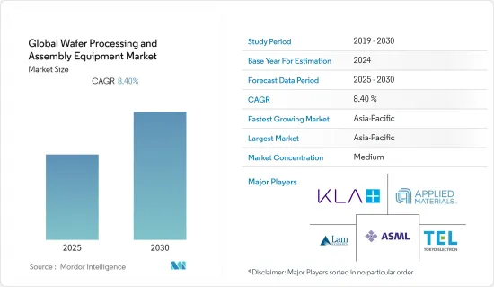
預測期內全球晶圓加工和組裝設備市場預計複合年成長率為 8.4%
關鍵亮點
- 根據印度品牌資產基金會的數據,印度家用電子電器和家用電子電器(ACE) 產業預計將以 9% 的複合年成長率成長,到 2022 年達到 3.15 兆印度盧比(約 483.7 億美元)。預計到 2024-25 年,印度電子製造業的規模將達到 3,000 億美元(22.5 兆印度盧比)。此外,預計家用電子電器的使用和消費增加將推動對半導體的需求,從而在整個預測期內推動晶圓加工和組裝設備市場的收益。
- 晶圓加工和組裝設備行業的一個突出趨勢是對更小晶圓和更高設備性能的需求不斷增加。例如,晶圓被平坦化到最終幾十微米的厚度。用於記憶體、CIS 和電源應用的半導體晶圓大多數都縮小到 100μm 至 200μm 的厚度。對於儲存設備而言,需要在單一封裝中最大化儲存容量,增加資料傳輸速度和電力消耗(尤其是在行動應用中),這些都推動著對更薄設備的需求。 2D NAND/DRAM 等標準儲存設備使用厚度超過 200μm 的晶圓。
- 該地區的政府機構正在計劃投資半導體生產,這可能為研究市場創造成長機會。例如,德國經濟部於2021年9月宣布,打算向歐盟的「歐洲通用利益重要計劃」計畫投資30億歐元。該計劃是歐盟刺激投資和減少進口依賴的主要補貼手段之一。這筆資金將由德國政府用於興建新的半導體製造廠。這項投資主要是為了減少未來半導體需求對進口半導體的依賴。預計此類政府措施將極大地推動所研究的市場。
- 在晶圓製造週期中,晶圓會因鋸切、手動處理、流體噴射、運輸系統和拾放設備而受到機械應力。目前商用的功率半導體一般是在200毫米晶圓上製造,厚度為50-100μm,但藍圖顯示它們可以做得薄至1μm。機械拋光使這些晶片的背面變薄。研磨痕跡、由於研磨不良而導致的邊緣缺口、星形裂紋、由於邊緣顆粒卡在研磨中而引起的彗星、嵌入顆粒、解理線和其它各種缺陷都是由拋光過程引起的缺陷。
- 此外,新冠疫情引發的全球半導體晶圓短缺,正促使參與企業集中精力提高產能。例如,中芯國際正制定積極計劃,到 2025 年透過在各個城市建設新的晶片製造廠,實現產能加倍,其中包括 2021 年 9 月宣布將在上海自貿區建立新工廠。
晶圓加工與組裝設備市場趨勢
薄膜沉澱是市場促進因素之一
- 化學氣相沉積(CVD)技術常用於半導體和薄膜的製造。 CVD設備市場的擴張主要得益於半導體、LED和儲存設備產業的快速成長,這是由於對微電子消費品的需求不斷增加,以及對Cr6用於電鍍的嚴格限制。
- 2022 年 1 月:韓國專業真空爐製造商 ThermVac Inc. 透過開發可在 900°C 至 2,400°C 溫度範圍內使用的 CVD 設備的製程技術以及設計和製造技術,繼續滿足國內外客戶的需求。這滿足了半導體、光伏、行動電話、航太和國防等高科技產業對耐高溫 CVD 組件日益成長的需求。
- 線性濺鍍系統用於太陽能、顯示器、資料儲存和半導體等應用。例如,2021年12月,博世開始量產基於SiC的功率半導體,供應全球汽車製造商。為了滿足對半導體日益成長的需求,2021 年,博世位於羅伊特林根的晶圓廠增加了 10,764 平方英尺的無塵室空間。預計到 2023年終將增加 32,292 平方英尺。預計半導體產量的成長將推動所研究市場的發展。
- 預計區域汽車行業的進步將為市場成長創造巨大機會。例如,杜拜最近發起了宣傳活動,到 2030 年,該酋長國的道路上將有 42,000 輛電動車。濺鍍設備用於塗覆動力傳動系統軸承和零件,而電動車新興市場的發展將成為該市場的主要驅動力。
- 濺鍍薄膜在生物醫學應用的應用越來越廣泛。其中一個例子是採用圓柱形磁控濺鍍在一批醫療支架上沉積保護塗層。奈米薄膜廣泛應用於電子、紡織、醫藥、陶瓷和許多其他應用領域。塗有奈米薄膜的織物通常透過化學沉澱、溶膠-凝膠或磁控濺鍍方法來生產。例如磁控濺鍍具有膜厚可控、純度高、速度快、溫度低、附著力優良、操作簡單、環境友善等優點。
亞太地區佔市場主要佔有率
- 亞太地區是全球成長最快的半導體市場。中國、韓國和新加坡等國家對智慧型手機和其他家用電子電器的強勁需求,促使許多供應商在該地區建立生產設施。
- 這些公司正在透過啟動新計劃來擴大其在該地區的業務,以滿足客戶的多樣化需求。例如,2021 年 9 月,UTAC Holding, Ltd. 在其先進的半導體製造解決方案套件中增加了尖端等離子切割和多計劃晶圓 (MPW) 功能。等離子切割可以縮小晶片之間的劃線寬度,從而增加每個晶圓上的晶片數量。它還可以實現「近乎完美」的切割質量,不會出現碎片和裂紋,這比可能導致長期側壁質量問題的傳統機械鋸切工藝具有明顯的優勢。
- 此外,上市私人公司都在投資新產品和研發設施。例如,2021 年 9 月,中國最大的晶片代工製造商中芯國際(SMIC)宣布與上海自貿區臨港特區達成協議。根據協議,中芯國際將建立一座月產能10萬片12吋晶圓的新晶圓廠。中芯國際也於 2021 年 3 月宣布,將與深圳市政府合作,投資 23.5 億美元建造一座製造工廠,生產 28 奈米(nm)及以上製程的積體電路,月產能為 40,000 片 12 吋晶圓。
- 同樣,2021 年 10 月,新南威爾斯州政府意識到全球半導體產業缺乏主要企業,並計劃建立一個新中心,以提高該領域關鍵工作的可行性。該中心名為半導體產業服務局 (S3B),位於雪梨科技中心,由州政府資助。此外,首席科學家和工程師辦公室在審查了國內半導體產業後表示,目前澳洲沒有以半導體設計或開發為核心業務的大型公司。新工廠將利用該國的晶圓加工和切割設備市場。
- 隨著矽通孔(TSV)技術在行動電話和其他無線及網路設備等低功耗、高效能設備中的應用越來越廣泛,對隱形切割設備的需求也日益增加。 TSV 允許進行 2.5/3D 封裝,使其適用於 TSV 組裝/封裝(透過隱形切割和其他製程進行晶片到晶片、晶片到晶圓的組裝)。對於記憶體和邏輯,採用雷射切割和刀片切割相結合的方式。
晶圓加工與組裝設備產業概況
全球晶圓加工和組裝設備市場適度整合。為了滿足每個行業不斷變化的需求,公司傾向於投資創新其產品。此外,參與企業正在採取夥伴關係、合併和收購等策略活動來擴大其影響力。近期市場發展趨勢如下:
- 2022年3月-SK siltron宣佈在美國密西根州貝城啟動碳化矽 (SiC) 半導體晶片製造廠。該公司計劃每年生產約6萬台。此外,6吋SiC晶圓將成為主力產品。
- 2021 年 9 月-英飛凌科技股份公司將在其位於奧地利的晶圓廠推出一個用於生產 300 毫米薄晶圓上的功率半導體元件的高科技晶片工廠。該投資額達16億歐元,將成為歐洲微電子領域最大的計劃之一。據該公司介紹,該工廠計劃的工業半導體年生產能力將足以為其配備光伏系統,總合可產生約 1,500 TWh 的電力,大約是德國年電力消耗量的三倍。
其他福利
- Excel 格式的市場預測 (ME) 表
- 3 個月的分析師支持
目錄
第 1 章 簡介
- 研究假設和市場定義
- 研究範圍
第2章調查方法
第3章執行摘要
第4章 市場洞察
- 市場概況
- 產業吸引力-波特五力分析
- 供應商的議價能力
- 買家的議價能力
- 新進入者的威脅
- 替代品的威脅
- 競爭對手之間的競爭
- 評估新冠肺炎對市場的影響
第5章 市場動態
- 市場促進因素
- 消費者需求不斷成長
電子設備需求不斷成長
製造業展望
- 人工智慧的傳播
人工智慧、物聯網和連網型設備
行業專用設備快速增加
- 市場問題
- 技術的動態本質
生產設備
生產設備
第6章 市場細分
- 依設備類型
- 化學機械拋光
(中國新聞網)
- 蝕刻
- 薄膜沉澱
- CVD
- 濺
- 其他
- 光阻劑處理
- 組裝設備
- 晶粒黏接
- 焊線
- 包裝
- 檢查和切割
電鍍等
- 按地區
- 亞太地區
- 北美洲
- 其他
- 依產品-晶圓加工設備
- DRAM
- NAND
- 選角/邏輯
- 其他
第7章:供應商排名分析
第8章 競爭格局
- 公司簡介
- Applied Materials Inc
- ASML Holding Semiconductor Company
- Tokyo Electron Limited
- Lam Research Corporation
- KLA Corporation
- Hitachi High-Technologies Corporation
- Disco Corporation
- ASM Pacific Technology
- Kulicke and Soffa Industries, Inc
- BE Semiconductor Industries NV
- Towa Corporation
第9章投資分析
第10章:投資分析市場的未來
The Global Wafer Processing and Assembly Equipment Market is expected to register a CAGR of 8.4% during the forecast period.
Key Highlights
- According to the Indian Brand Equity Foundation, In 2022, the Indian appliance and consumer electronics (ACE) sector is predicted to grow at a 9% compound annual growth rate (CAGR) to INR 3.15 trillion (USD 48.37 billion). The Indian electronics manufacturing sector is expected to reach USD 300 billion (INR 22.5 lakh crore) by 2024-25. Furthermore, increased consumer electronics device usage and consumption are predicted to fuel semiconductor demand, boosting wafer processing and assembly equipment market revenues throughout the projection period.
- A prominent trend in the wafer processing and assembly equipment industry is the growing demand for miniaturized wafers with higher device performance. Wafers, for example, are flattened down to final thicknesses of tens of micrometers. Most semiconductor wafers used in memory, CIS, and power applications are reduced to 100 µm-200 µm in thickness. In the case of memory devices, further thickness reduction is required due to the need to maximize the memory capacity of single packages, increased data transmission rates, and power consumption fueled mostly by mobile applications. Silicon wafers thicker than 200 µm are used in standard memory devices like 2D NAND/DRAM.
- The government bodies in the different regions are planning to invest in the production of semiconductors, which may create an opportunity for the studied market to grow. For instance, in September 2021, Germany's economy ministry stated that the country is willing to invest EUR 3 billion in the EU's "Important Projects of Common European Interest" initiative, which is one of the EU's primary subsidy tools for stimulating investment and reducing import dependency. The money will be used by the German government to build new semiconductor manufacturing factories. This investment is primarily aimed at reducing dependency on imported semiconductors for future semiconductor needs. Government policies like this will significantly drive the studied market.
- Wafers are subjected to mechanical loads induced by sawing, manual handling, liquid jets, transport systems, and pick and place equipment during the wafer manufacturing cycle. Power semiconductors on the market now are generally made on 200-mm wafers with thicknesses ranging from 50 to 100 µm, although their roadmaps allow for wafers as thin as 1 µm. Mechanical polishing thins the backside of these wafers. Grinding marks, grinding failures resulting in edge chips, star cracks, and comets generated by edge particles caught in the grinding wheel, embedded particles, cleavage lines, and a variety of other faults are all defects caused by the polishing process.
- Furthermore, the global shortage of wafer semiconductors led by the COVID-19 pandemic has encouraged players to focus on increasing production capacity. For instance, Semiconductor Manufacturing International Corp (SMIC) has indulged in aggressive plans to double its production capacity by 2025 by constructing new chip fabrication plants in different cities, including its announcement in September 2021 to establish a new factory in Shanghai's free trade zone.
Wafer Processing & Assembly Equipment Market Trends
Thin Film Deposition is One of the Factor Driving the Market
- The Chemical Vapor Deposition (CVD) technology is commonly employed in the fabrication of semiconductors and thin films. The expansion of the CVD equipment market is primarily driven by increasing demand for microelectronics-based consumer items, which is resulting in quicker growth of the semiconductor, LED, and storage device industries, as well as severe limits on the use of Cr6 for electroplating.
- In January 2022, ThermVac Inc., a Korean manufacturer of special vacuum furnaces, continues to respond to the needs of domestic and international clients by developing process technology and design and manufacturing technology for CVD equipment that can be used at temperatures ranging from 900°C to 2,400°C. This corresponds to the growing demand for high-temperature heat-resistant CVD components in high-tech industries like semiconductors, solar power, mobile phones, aerospace, and defense.
- The linear sputtering equipment is used in applications like solar energy, display, Data storage, semiconductor, and many more. For instance, in December 2021, Bosch started the volume production of Sic-based power semiconductors supplying automotive manufacturers worldwide. To meet the increasing demand for such semiconductors, an extra 10,764 square feet were already added to the clean-room space at the Bosch wafer fab in Reutlingen in 2021. Another 32,292 square feet will be added by the end of 2023. Such an increase in the production of semiconductors will drive the studied market.
- The advancements in the regional automotive industry are expected to create significant opportunities for market growth. For instance, Dubai recently launched a campaign to have 42,000 EVs on the streets of Emirates by 2030. The sputtering equipment is used in the coating of Drive train bearings and components as the increase in the developments of EV vehicles will significantly drive the studied market.
- Sputtered thin films are increasingly being used in biomedical applications. An example is a cylindrical magnetron sputtering to deposit protective coatings on batches of medical stents. Nano-films are widely employed in electronics, textiles, pharmaceuticals, ceramics, and various other applications. Fabrics coated with Nanofilm are often created by chemical vapor deposition, sol-gel technique, and magnetron sputtering. The magnetron sputtering method, for example, offers the benefits of controlled film thickness, high purity, high speed and low temperature, excellent adhesion, ease of operation, and environmental friendliness, among others.
Asia Pacific Holds the Major Share of the Market
- Asia-Pacific has the world's fastest-growing semiconductor market. Many vendors are setting up production facilities in the region in response to strong demand for smartphones and other consumer electronics gadgets from nations including China, the Republic of Korea, and Singapore.
- The companies are expanding their presence in the region by starting new projects to cater to the wide need of the customer. For instance, in September 2021, UTAC Holding, Ltd. added state-of-the-art plasma dicing and multi-project wafer (MPW) capabilities to a range of advanced semiconductor manufacturing solutions. Plasma dicing narrows the scribe line width between chips and increases the number of chips per wafer. Also, it provides "nearly perfect" cutting quality with no chips or cracks, which is a clear advantage over traditional mechanical sawing processes that lead to chronic sidewall quality issues.
- Further public agencies and private companies are investing in new products and research & development facilities. For instance, In September 2021, China's largest contract chipmaker Semiconductor Manufacturing International Corp (SMIC) announced the company's agreement with the Lin-Gang Special area-part of Shanghai's free trade zone. This agreement enables SMIC to establish a new foundry with a monthly planned capacity of 100,000 12-inch wafers. Also, in March 2021, the company announced an investment of USD 2.35 billion in coordination with the Shenzhen government for a manufacturing facility to produce 28nanometre (nm) and above integrated circuits with a monthly capacity of 40,000 12-inch wafers.
- Similarly, in October 2021, the Government of New South Wales is aware that the global semiconductor industry lacks Australia's major players and plans a new center to improve the feasibility of critical jobs in this sector. The hub, the Semiconductor Sector Service Bureau (S3B), will be based in Sydney's Tech Central and be funded by the state government. Further, Chief Scientist and Engineer Office, after researching the national semiconductor scene, mentioned there are currently no major Australian companies with semiconductor design or semiconductor development as their core business. The new hub leverages the country's wafer processing and dicing equipment market.
- The demand for stealth dicing equipment is growing as TSV (Through Silicon Via) technology becomes more prevalent for low-power, high-performance devices such as mobile phones and other wireless and networking devices. As TSV can package 2.5/3D for the applications listed above, the equipment is useful for TSV Assembly/Packaging (chip-to-chip and chip-to-wafer assembly with stealth dicing and other processes). In Memory and Logic, a combination of laser dicing and blade dicing is used.
Wafer Processing & Assembly Equipment Industry Overview
The Global Wafer Processing and Assembly Equipment market is moderately consolidated. Players tend to invest in innovating their product offerings to cater to the different industry's changing demands. Moreover, players adopt strategic activities like partnerships, mergers, and acquisitions to expand their presence. Some of the recent developments in the market are:
- March 2022 - SK siltron announced the beginning of the operation of the Silicon carbide (SiC) semiconductor wafer manufacturing plant in Bay City, Michigan, US. The company has a plan to produce around 60,000 annually. Also, a 6-inch SiC wafer is the main product of the company.
- September 2021 - Infineon Technologies AG launched its high-tech chip factory for power semiconductor devices on 300-millimeter thin wafers at its Villach site in Austria. At EUR 1.6 billion, the investment made by the company represents one of the largest such projects in the microelectronics sector in Europe. According to the company, the annual capacity planned for industrial semiconductors from the facility is sufficient to equip solar systems producing a total of around 1,500 TWh of electricity, which is around three times the annual power consumption of Germany.
Additional Benefits:
- The market estimate (ME) sheet in Excel format
- 3 months of analyst support
TABLE OF CONTENTS
1 INTRODUCTION
- 1.1 Study Assumption And Market Defination
- 1.2 Scope of the study
2 RESEARCH METHODOLOGY
3 EXECUTIVE SUMMARY
4 MARKET INSIGHTS
- 4.1 Market Overview
- 4.2 Industry Attractiveness - Porter's Five Forces Analysis
- 4.2.1 Bargaining Power Of Suppliers
- 4.2.2 Bargaining Power Of Buyers
- 4.2.3 Threat Of New Entrants
- 4.2.4 Threat Of Substitutes
- 4.2.5 Intensity Of Competitive Rivalry
- 4.3 Assessment of the Impact of Covid-19 on the Market
5 MARKET DYNAMICS
- 5.1 Market Drivers
- 5.1.1 Increasing Needs of Consumer
Electronic Devices Boosting the
Manufacturing Prospects
- 5.1.2 Proliferation of Artificial
Intelligence, IoT and Connected
Devices across Industry Verticals
- 5.2 Market Challenges
- 5.2.1 Dynamic Nature of Technologies
Requires Several Changes in
Manufacturing Equipment
6 MARKET SEGMENTATION
- 6.1 By Equipment Type
- 6.1.1 Chemical Mechanical Polishing
(CMP)
- 6.1.2 Etching
- 6.1.3 Thin Film Deposition
- 6.1.3.1 CVD
- 6.1.3.2 Sputter
- 6.1.3.3 Other Type
- 6.1.4 Photoresist Processing
- 6.1.5 Assembly Equipment
- 6.1.5.1 Die Attach
- 6.1.5.2 Wire Bonding
- 6.1.5.3 Packaging
- 6.1.5.4 Inspection, Dicing,
Plating and Others
- 6.2 By Geography
- 6.2.1 Asia-Pacific
- 6.2.2 North America
- 6.2.3 Rest of the World
- 6.3 By Product - Wafer Processing Equipment
- 6.3.1 DRAM
- 6.3.2 NAND
- 6.3.3 Foundry/Logic
- 6.3.4 Other Products
7 VENDOR RANKING ANALYSIS
8 COMPETITIVE LANDSCAPE
- 8.1 Company Profiles
- 8.1.1 Applied Materials Inc
- 8.1.2 ASML Holding Semiconductor Company
- 8.1.3 Tokyo Electron Limited
- 8.1.4 Lam Research Corporation
- 8.1.5 KLA Corporation
- 8.1.6 Hitachi High-Technologies Corporation
- 8.1.7 Disco Corporation
- 8.1.8 ASM Pacific Technology
- 8.1.9 Kulicke and Soffa Industries, Inc
- 8.1.10 BE Semiconductor Industries N.V
- 8.1.11 Towa Corporation
9 INVESTMENT ANALYSIS
10 FUTURE OF THE MARKET
 單晶圓加工設備市場:依製程、晶圓尺寸、技術節點及應用分類-2026年至2032年全球預測
 薄晶圓加工和切割設備市場分析及預測(至2035年):按類型、產品類型、服務、技術、組件、應用、材料類型、製程、最終用戶和設備分類
 2026年全球晶圓加工設備市場報告
 晶圓加工設備市場-全球產業規模、佔有率、趨勢、機會、預測:按製程、應用、最終用戶、地區和競爭對手分類,2021-2031年
 薄晶圓加工切割設備市場機會、成長要素、產業趨勢分析及2026年至2035年預測
 全球晶圓切割服務市場:依材料、尺寸、切割技術與地區劃分 - 市場預測與分析 (2026-2035)
 薄磚市場:按產品類型、材料類型、應用和地區分類
 晶圓加工與組裝設備市場-2025年至2030年預測雷射開槽設備市場(按雷射類型、操作類型、雷射功率容量、技術、應用和最終用戶分類)—2025-2030 年全球預測
 薄晶圓加工和切割設備:市場佔有率分析、行業趨勢和成長預測(2025-2030)