


 |
市場調查報告書
商品編碼
1687405
薄晶圓加工和切割設備:市場佔有率分析、行業趨勢和成長預測(2025-2030)Thin Wafer Processing And Dicing Equipment - Market Share Analysis, Industry Trends & Statistics, Growth Forecasts (2025 - 2030) |
||||||
※ 本網頁內容可能與最新版本有所差異。詳細情況請與我們聯繫。
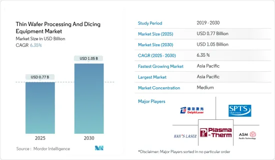
薄晶圓加工和切割設備市場規模預計在 2025 年為 7.7 億美元,預計到 2030 年將達到 10.5 億美元,預測期內(2025-2030 年)的複合年成長率為 6.35%。
主要亮點
- 隨著電子元件使用量不斷增加,人們對電子封裝的需求也越來越大,要求電子封裝更加資源豐富,以適應各種應用。這些因素正在推動半導體和IC封裝市場的成長。
- 預計未來幾年推動薄晶圓加工和切割設備需求的主要因素之一是3D積體電路的需求不斷成長,3D積體電路廣泛應用於記憶卡、智慧型手機、智慧卡和各種運算設備等微型半導體設備。
- 3D電路在一些空間受限的應用中變得越來越普遍,包括攜帶式消費性電子產品、感測器、MEMS 和工業產品,以提高整體產品性能,包括更快的速度、耐用性、更低的功耗和更輕的記憶體。
- 低成本雲端處理解決方案的普及正在推動企業和產業對伺服器和資料中心系統的使用增加,這可能會增加對微處理器和數位訊號處理器等邏輯設備的需求。此外,隨著越來越多支援物聯網的連接設備的出現,微處理器的使用也增加。這些設備擴大使用薄晶圓來實現有效的熱管理並提高性能。這些因素正在推動市場成長。
- 多年來,矽晶片一直被用作微電子和 MEMS 的製造平台。絕緣體上矽基基板是標準矽晶片的獨特變體。使用約 1-2 μm 厚的二氧化矽鍵結層將兩片晶圓結合在一起,形成晶圓。每個晶圓被平整化至10-50μm的厚度。塗層的具體厚度取決於應用。
- 建造一座最先進的薄晶圓代工廠的成本正在指數級成長,給市場帶來壓力。近期,半導體製造商的數量正在不斷整合。性能改進正在放緩,使得專用薄晶圓更具吸引力。允許薄晶圓通用的設計決策可能並不適用於某些計算任務。
- 半導體研究的各種發展正在為市場創造更多機會。例如,2023年4月,Lapidus正式加入Imec核心合作夥伴計劃,在與Imec在先進半導體研究領域的永續合作方面邁出了重要一步。此舉加強了該公司對半導體領域長期合作和進步的承諾。
薄晶圓加工切割設備市場趨勢
半導體小型化需求的不斷成長推動了市場
- 根據美國消費科技協會預測,2022年至2024年間,美國美國電子產品零售額將小幅成長,總額將超過5,000億美元。預計這將增加開發電子產品對晶圓的需求。與醫療保健和汽車半導體 IC 製造商等其他終端使用者一樣,消費性電子產品的需求也迫使 IC 小型化。這將導致市場小型化程度的提高,並有望在預測期內推動需求。
- 從地區來看,無晶圓廠經營模式是亞洲國家在全球半導體銷售中佔據突出地位的主要因素。無廠半導體公司通常委託製造外包給純代工廠或外包裝組裝和測試 (OSAT) 公司。
- FUJIFILM表示,隨著人工智慧、物聯網、下一代通訊標準「5G」的廣泛應用以及自動駕駛技術的進步,對半導體的需求和性能預計會不斷提高,半導體設備的小型化仍在繼續。這些因素推動了對小型、輕量消費設備的需求,這些設備依靠建立在超薄矽晶片上的3D電路架構來實現最佳效能。
- 這種晶圓極為薄且平坦。同時,小型化也帶來了將多種功能整合到單一晶片上的需求。直徑12吋的更大晶圓正在引領晶圓技術的新趨勢。
- 2023年12月,三星電子與ASML Holding NV宣布將共同投資7.6億美元在韓國建立先進的研發設施。該設施的主要目的是增強半導體製造程序,特別注重利用 ASML 的尖端 EUV 技術。這項策略性夥伴關係關係至關重要,因為三星計劃在前一年成功量產 3μm 晶片後,到 2025 年實現 2 奈米晶片的商業化。
預計亞太地區將佔據最大市場佔有率
- 亞太地區是全球最大且成長最快的半導體市場。中國、韓國和新加坡等國家對智慧型手機和其他消費性電子設備的龐大需求促使許多供應商在當地建立製造工廠。
- 中國各市場公司正致力於透過收購和合併來擴大業務。例如,2023年12月,一家中國半導體設計公司與一家馬來西亞晶片封裝公司合作組裝高階圖形處理單元(GPU)。由中國華天科技控股的友尼森公司和其他馬來西亞晶片封裝公司注意到來自中國合作夥伴的業務和諮詢增加。 Xfusion 和 StarFive 等中國公司曾計劃在馬來西亞擴張。
- 鑑於全球半導體產業不斷變化的動態,越南和印度等其他國家也在尋求成為晶片製造服務的替代者。這一轉變表明,中國企業選擇在海外組裝晶片,從而降低了地緣政治風險,並使其更容易進入海外市場。
- 日本是半導體產業不可或缺的一部分,因為它是幾家主要製造商和電子產業的所在地。預計政府將調查大型晶片製造商進入該國的可能性。同時,日本企業被視為半導體製造和封裝中最關鍵材料的主要供應商。對於日本供應商而言,日本外匯和高製造成本使得材料價格更高,從而為其他低階應用供應商創造了機會。
- 澳洲的電子製造業正在蓬勃發展,各個終端用戶產業擴大採用先進設備來影響市場的成長。家電產品的成長主要得益於電視和智慧型手機的銷售。
- 2023 年 12 月,雪梨大學奈米研究所推出了一款設計類似樂高積木且頻寬更高的新晶片。這種緊湊的矽半導體晶片無縫地結合了電子和光子元件。這項突破性技術顯著提高了射頻(RF)頻寬,並提高了晶片內資訊管理的精度。該晶片利用先進的矽光電技術,能夠在寬度不到五毫米的空間內整合各種半導體系統。
- 全自動駕駛汽車的成長軌跡將在很大程度上受到亞太地區因素的影響,包括技術進步、消費者接受全自動駕駛汽車的意願、定價以及供應商和OEM解決汽車安全關鍵問題的能力。由於這些因素,汽車和半導體行業不斷專注於提高技術、協商原料價格以及為汽車配備可靠的技術。
薄晶圓加工切割設備產業概況
薄晶圓加工和切割設備市場呈現半固體,僅由 Disco、 Panasonic、Nippon Pulse Motor 和 Taiwan Pulse 馬達等少數幾家大公司組成。薄晶圓製造製程市場仍面臨重大挑戰。由於上述因素,新進入者進入市場的速度較慢。然而,市場上企業不斷的技術創新和研發努力幫助他們保持競爭優勢。因此,市場競爭對手之間的競爭處於中等水平。
- 2024 年 3 月:日立高科技宣布推出新系統 LS9300AD,該系統可檢查無圖案晶圓的正面和背面是否有顆粒和缺陷。除了使用傳統的暗場雷射散射法檢測異物和缺陷外,LS9300AD 還配備了新的 DIC(微分乾涉對比)檢測功能,可以檢測淺的、低縱橫比的、微小的不均勻缺陷。 LS9300AD採用了傳統產品中的晶圓邊緣夾持方式和旋轉台,可以檢查晶圓的正面和背面。
- 2023 年 11 月,康寧將其德國雷射技術業務出售給中國蘇州德爾福雷射。在此次交易中,蘇州德爾福雷射收購了康寧雷射技術部門的全部股份。
其他福利:
- Excel 格式的市場預測 (ME) 表
- 3個月的分析師支持
目錄
第1章 引言
- 研究假設和市場定義
- 研究範圍
第2章調查方法
第3章執行摘要
第4章 市場洞察
- 市場概覽
- 產業吸引力波特五力分析
- 新進入者的威脅
- 買家的議價能力
- 供應商的議價能力
- 替代品的威脅
- 競爭對手之間的競爭強度
- 產業價值鏈分析
- COVID-19 的副作用和其他宏觀經濟因素將如何影響市場
第5章市場動態
- 市場促進因素
- 對智慧卡、RFID 技術和汽車電源 IC 的需求不斷成長
- 半導體小型化需求日益成長
- 市場限制
- 製造挑戰
第6章市場區隔
- 依設備類型
- 薄膜裝置
- 切割設備
- 刀片切割
- 雷射消熔
- 隱形切割
- 等離子切割
- 按應用
- 記憶體/邏輯 (TSV)
- MEMS元件
- 功率元件
- CMOS影像感測器
- RFID
- 其他
- 按晶圓厚度
- 750微米
- 120微米
- 50微米
- 按晶圓尺寸
- 4英吋或更小
- 5英寸和6英寸
- 8吋
- 12英吋
- 按地區
- 北美洲
- 歐洲
- 亞洲
- 澳洲和紐西蘭
- 拉丁美洲
- 中東和非洲
第7章競爭格局
- 公司簡介
- Suzhou Delphi Laser Co. Ltd
- SPTS Technologies Limited
- Plasma-Therm LLC
- Han's Laser Technology Industry Group Co. Ltd
- ASM Laser Separation International(ALSI)BV
- Disco Corporation
- Tokyo Seimitsu Co, Ltd(Accretech)
- Neon Tech Co. Ltd
- Advanced Dicing Technologies Ltd
- Panasonic Corporation
- Hitachi High-Tech Corporation
第8章投資分析
第9章 市場機會與未來趨勢
The Thin Wafer Processing And Dicing Equipment Market size is estimated at USD 0.77 billion in 2025, and is expected to reach USD 1.05 billion by 2030, at a CAGR of 6.35% during the forecast period (2025-2030).
Key Highlights
- The increasing efforts to make electronic packaging highly resourceful due to the enormous demand for electronic components owing to amplified usage have made electronic packaging useful in a myriad of applications. These factors are driving the growth of the semiconductor and IC packaging market.
- One of the major factors expected to boost the demand for thin wafer processing and dicing equipment in the coming years is the growing demand for three-dimensional integrated circuits, which are widely used in miniature semiconductor devices such as memory cards, smartphones, smart cards, and various computing devices.
- Three-dimensional circuits are becoming more popular in multiple space-constrained applications, such as portable consumer electronics, sensors, MEMS, and industrial products because they improve overall product performance in terms of speed, durability, low power consumption, and lightweight memory.
- Due to the widespread availability of low-cost cloud computing solutions, the expanding use of server and data center systems across various enterprises and industries is likely to fuel demand for logic devices like microprocessors and digital signal processors. In addition, as the number of IoT-enabled linked devices grows, the utilization of microprocessors also increases. Thin wafers are increasingly employed in these devices to enable effective temperature management and enhance performance. Such factors are responsible for the growth of the market.
- Silicon wafers have long been used as a fabrication platform in microelectronics and MEMS. The silicon-on-insulator substrate is a unique variation of the standard silicon wafer. Two silicon wafers are glued together using a bond layer of silicon dioxide with a thickness of about 1-2 μm to make these wafers. One silicon wafer gets flattened down to 10-50 μm in thickness. The application will determine the exact thickness of the coating.
- The cost of building state-of-the-art thin wafer foundries has increased exponentially, which puts pressure on the market. The number of semiconductor manufacturers has consolidated in recent times. Performance boosts are slowing down, making specialized thin wafers increasingly attractive. The design decisions that enable thin wafers to be universal may be sub-optimal for some computing tasks.
- Various developments in semiconductor research further create opportunities for the market. For instance, in April 2023, Rapidus officially joined Imec's Core Partner Program, marking a significant stride in sustainable collaboration with Imec in advanced semiconductor research. This move reinforced their commitment to long-term collaboration and advancement in the semiconductor domain.
Thin Wafer Processing And Dicing Equipment Market Trends
Increasing Need for Miniaturization of Semiconductors is Expected to Drive the Market
- According to the Consumer Technology Association, in the US, retail sales of consumer electronics were expected to grow marginally between 2022 and 2024, with the total value exceeding USD 500 billion. This would increase the demand for wafers to develop electronic products. The demand for consumer electronics products, along with other end users such as healthcare and automotive semiconductor IC manufacturers, is forcing them to reduce the size of ICs. It has, therefore, given rise to miniaturization in the market, which is expected to experience a surge in its demand during the forecast period.
- Across geographies, the fabless business model is the major contributor to the prominent position of various Asian countries in semiconductor sales worldwide. Fabless firms typically outsource fabrication to pure-play foundries and outsourced assembly and test (OSAT) firms.
- According to Fujifilm, the miniaturization of semiconductor devices continues as the increasing use of AI, IoT, and next-generation communication standard '5G' and the advancement of autonomous driving technology are expected to increase the demand for and performance of semiconductors. The factors mentioned above have led to the rise in demand for small and lightweight consumer devices that rely on 3D circuit architecture built onto ultra-thin silicon wafers in order to perform at peak capacity.
- These wafers are extremely thin and flat. At the same time, miniaturization has resulted in the need to integrate several features on a single chip. Due to large-sized wafers (with a diameter of up to 12 inches), there is a new trend in wafer technology.
- In December 2023, Samsung Electronics and ASML Holding NV announced a collaborative investment of USD 760 million to establish an advanced Research and Development (R&D) facility in South Korea. The primary objective of this facility is to enhance semiconductor manufacturing processes, with a specific focus on utilizing ASML's cutting-edge EUV technology. This strategic partnership is crucial for Samsung's goal of commercializing 2-nanometer chips by 2025, building on the successful mass production of 3 µm chips in the preceding year.
Asia-Pacific is Expected to Hold the Largest Market Share
- The Asia-Pacific is the largest and fastest-growing semiconductor market in the world. Significant demand for smartphones and other consumer electronics devices from countries such as China, the Republic of Korea, and Singapore encourages many vendors to set up regional production establishments.
- China's various market players are focusing on expanding business through acquisitions and mergers. For instance, in December 2023, Chinese semiconductor design companies teamed up with Malaysian chip packaging firms to assemble high-end graphics processing units (GPUs). Unisem, the majority of which is owned by China's Huatian Technology, and other Malaysian chip packaging companies noticed an uptick in business and inquiries from their Chinese partners. Companies like Xfusion and StarFive from China planned to expand their operations in Malaysia.
- Given the changing dynamics in the global semiconductor industry, other countries like Vietnam and India are also trying to become alternatives for chip manufacturing services. This shift shows that Chinese companies are choosing to assemble their chips outside China, reducing geopolitical risks and making it easier to reach markets outside the country.
- Japan occupies an essential position in the semiconductor industry as it is home to several major manufacturers and the electronics industry. The government is expected to investigate the potential for bringing major chip makers into the country. Meanwhile, Japanese organizations are considered significant suppliers of the most critical materials consumed in semiconductor manufacturing and packaging. For Japanese suppliers, Japanese exchange rates and high production costs make materials more expensive and open up opportunities for other suppliers for low-end applications.
- The growing electronics manufacturing sector in Australia and the increasing adoption of advanced devices among various end-user industries influence market growth. The sales of televisions and smartphones have primarily driven the increase in consumer electronics.
- In December 2023, the University of Sydney Nano Institute unveiled a new chip designed like LEGO blocks, featuring improved bandwidth. This compact silicon semiconductor chip smoothly combines electronics with photonic components. The breakthrough will significantly increase radio-frequency (RF) bandwidth and enhance the precision of managing information within the chip. Utilizing advanced silicon photonics technology, the chip has integration capabilities for various semiconductor systems, all within a width of less than 5 millimeters.
- The growth trajectory of fully autonomous automobiles is heavily influenced by factors in Asia-Pacific, including technology advancements, consumer willingness to accept fully automated vehicles, pricing, and suppliers' and OEMs' capacity to address significant concerns about vehicle safety. According to these factors, the automotive and semiconductor industries always concentrate on enhancing technologies, negotiating raw material prices, and combining cars with reliable technology.
Thin Wafer Processing And Dicing Equipment Industry Overview
The market for thin wafer processing and dicing is semi-consolidated and comprises very few major players, such as Disco Corporation, Panasonic Corporation, Nippon, and Pulse Motor Taiwan. The market still faces considerable challenges in the manufacturing processes of thin wafers. The above-mentioned factor has led to a slower entry of new players into the market. Nevertheless, the constant innovations and R&D efforts of market players help maintain a competitive edge. Therefore, competitive rivalry in the market is moderate.
- March 2024: Hitachi High-Tech Corporation announced the launch of the LS9300AD, a new system for inspecting the front and back sides of non-patterned wafer surfaces for particles and defects. In addition to the conventional dark-field laser scattering detection of foreign material and defects, the LS9300AD is equipped with a new DIC (Differential Interference Contrast) inspection function that enables the detection of irregular defects, even shallow, low-aspect microscopic defects. LS9300AD has the wafer edge grip method and rotating stage used in conventional products to enable front and backside wafer inspection.
- November 2023: Corning Inc. sold its German laser technology business to Suzhou Delphi Laser in China. The agreement involved Suzhou Delphi Laser acquiring the complete stake in the division known as Corning Laser Technologies.
Additional Benefits:
- The market estimate (ME) sheet in Excel format
- 3 months of analyst support
TABLE OF CONTENTS
1 INTRODUCTION
- 1.1 Study Assumptions and Market Definition
- 1.2 Scope of the Study
2 RESEARCH METHODOLOGY
3 EXECUTIVE SUMMARY
4 MARKET INSIGHTS
- 4.1 Market Overview
- 4.2 Industry Attractiveness Porter's Five Forces Analysis
- 4.2.1 Threat of New Entrants
- 4.2.2 Bargaining Power of Buyers
- 4.2.3 Bargaining Power of Suppliers
- 4.2.4 Threat of Substitute Products
- 4.2.5 Intensity of Competitive Rivalry
- 4.3 Industry Value Chain Analysis
- 4.4 Impact of COVID-19 Aftereffects and Other Macroeconomic Factors on the Market
5 MARKET DYNAMICS
- 5.1 Market Drivers
- 5.1.1 Increasing Demand for Smart Cards, RFID Technology, and Automotive Power ICs
- 5.1.2 Increasing Need for Miniaturization of Semiconductors
- 5.2 Market Restraint
- 5.2.1 Manufacturing Challenges
6 MARKET SEGMENTATION
- 6.1 By Equipment Type
- 6.1.1 Thinning Equipment
- 6.1.2 Dicing Equipment
- 6.1.2.1 Blade Dicing
- 6.1.2.2 Laser Ablation
- 6.1.2.3 Stealth Dicing
- 6.1.2.4 Plasma Dicing
- 6.2 By Application
- 6.2.1 Memory and Logic (TSV)
- 6.2.2 MEMS Devices
- 6.2.3 Power Devices
- 6.2.4 CMOS Image Sensors
- 6.2.5 RFID
- 6.2.6 Others
- 6.3 By Wafer Thickness
- 6.3.1 750 micrometers
- 6.3.2 120 micrometers
- 6.3.3 50 micrometers
- 6.4 By Wafer Size
- 6.4.1 Less than 4 inches
- 6.4.2 5 inches and 6 inches
- 6.4.3 8 inches
- 6.4.4 12 inches
- 6.5 By Geography
- 6.5.1 North America
- 6.5.2 Europe
- 6.5.3 Asia
- 6.5.4 Australia and New Zealand
- 6.5.5 Latin America
- 6.5.6 Middle East and Africa
7 COMPETITIVE LANDSCAPE
- 7.1 Company Profiles
- 7.1.1 Suzhou Delphi Laser Co. Ltd
- 7.1.2 SPTS Technologies Limited
- 7.1.3 Plasma-Therm LLC
- 7.1.4 Han's Laser Technology Industry Group Co. Ltd
- 7.1.5 ASM Laser Separation International (ALSI) BV
- 7.1.6 Disco Corporation
- 7.1.7 Tokyo Seimitsu Co, Ltd (Accretech)
- 7.1.8 Neon Tech Co. Ltd
- 7.1.9 Advanced Dicing Technologies Ltd
- 7.1.10 Panasonic Corporation
- 7.1.11 Hitachi High-Tech Corporation
8 INVESTMENT ANALYSIS
9 MARKET OPPORTUNITIES AND FUTURE TRENDS
 全球雷射開槽設備市場按雷射類型、製程類型、操作類型、產出能力、應用和最終用途行業分類 - 預測 2025-2030 年
 薄晶圓加工和切割設備市場,按產品類型、晶圓尺寸、晶圓厚度、應用、最終用戶、國家和地區分類 - 2025 年至 2032 年全球行業分析、市場規模、市場佔有率和預測
 晶圓加工設備市場 - 全球產業規模、佔有率、趨勢、機會和預測,按製程、應用、最終用戶、地區和競爭細分,2020-2030 年預測
 晶圓加工和組裝設備全球市場:市場佔有率分析、行業趨勢和統計、成長預測(2025-2030 年)
 晶圓處理設備的全球市場:市場規模·佔有率·趨勢,產業分析 (各工程·各用途·各終端用戶·各地區),未來預測 (2025年~2034年)晶圓加工設備市場:按產品類型、應用、最終用戶、技術節點分類 - 2025-2030 年全球預測單晶圓加工設備市場:按設備類型、應用、技術和最終用戶 - 2025-2030 年全球預測
 薄晶圓加工和切割設備市場機會、成長促進因素、產業趨勢分析與預測 2024 - 2032 年晶圓加工設備市場規模、佔有率、趨勢分析報告:按製程、按應用、按地區、細分市場預測,2024-2030
 晶圓雷射拉霸機市場預測至 2030 年:按類型、晶圓尺寸、應用、最終用戶和地區進行的全球分析