


 |
市場調查報告書
商品編碼
1685905
半導體封裝:市場佔有率分析、產業趨勢與統計、成長預測(2025-2030 年)Semiconductor Packaging - Market Share Analysis, Industry Trends & Statistics, Growth Forecasts (2025 - 2030) |
||||||
※ 本網頁內容可能與最新版本有所差異。詳細情況請與我們聯繫。
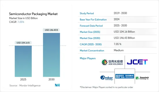
半導體封裝市場規模預計在 2025 年為 1,041.6 億美元,預計到 2030 年將達到 1,464.3 億美元,預測期內(2025-2030 年)的複合年成長率為 7.05%。
半導體封裝是指塑膠、陶瓷、金屬或玻璃製成的外殼,內含一個或多個離散半導體裝置或積體電路。封裝對於保護電子系統免受高頻噪音輻射、靜電放電、機械損壞和冷卻至關重要。
高效能運算、資料中心網路和自動駕駛汽車正在推動該市場的採用率並加速技術進步。目前趨勢是雲端運算、邊緣運算和設備層面擁有更多的運算資源。此外,通訊業和基礎設施產業的高階性能應用和人工智慧(AI)的成長也推動了所研究市場的發展。
隨著前端節點的縮小,設計成本變得越來越重要。先進封裝 (AP) 解決方案透過提高系統效能同時降低成本、提供更低的延遲、更高的頻寬和更高的功率效率來幫助解決這些問題。
職場的數位化位化、遠端工作和遠端工作趨勢的出現以及消費者對電子設備日益成長的偏好,正在推動對半導體設備的需求,從而可以釋放廣泛的新機會。隨著半導體裝置的成長不斷加速,先進的封裝技術提供了數位化時代所需的尺寸和處理能力。
世界各國政府正透過降低門檻、增加生產和研發補貼等方式加大對半導體產業的支持。例如,韓國承諾投入高達 4,560 億美元的私人投資來打造全球最大的晶片中心,彰顯其主導該產業的雄心壯志。
同時,韓國政府推出大規模扶持半導體產業措施,總額高達26兆韓元(約191億美元)。該計劃涵蓋財政援助、基礎設施建設、研發和對中小企業的針對性支持。韓國目前正在首爾郊外建造一個“巨型晶片叢集”,預計將成為全球最大的半導體中心,並成為創造許多新的就業機會的關鍵驅動力。
設計、開發和安裝半導體封裝設備以滿足汽車、家電、醫療保健、IT 和通訊、航太和國防等各行業的需求,需要大量的前期投資。這可能會限制半導體封裝市場的成長。
此外,每個國家的國防預算都受到通貨膨脹、經濟成長、政府支出重點以及全球貿易和地緣政治動態等關鍵宏觀經濟因素的影響。
2023年3月,拜登總統提案了美國史上最大的和平時期國防預算,總額達8,860億美元。該預算包括士兵薪資增加5.2%以及創紀錄的研發累計。在俄羅斯在烏克蘭採取行動的背景下,增加軍事裝備支出的必要性進一步凸顯。
根據美國預算辦公室預測,美國國防支出將持續增加,直至2033年。 2023年,美國國防支出預計將達7,460億美元,到2033年將增加至1.1兆美元。
半導體封裝市場趨勢
通訊和電訊業作為最終用戶正在快速成長
- 網路和連接性的演變是顯而易見的。我們已經從透過有線基礎設施進行語音和視訊訊號的基本交換發展到目前透過無線基礎設施進行多媒體和大量資料的交換。
- 半導體在通訊基礎設施中至關重要,處理從資料擷取和編碼到加密、傳輸以及最終呈現給使用者的各種任務。 5G 技術預示著 IT 和通訊網路及設備的重大飛躍,提供更快的速度和重點的極低延遲。這種降低的延遲對於雲端遊戲和 VR 內容流等應用尤其重要。因此,通訊和通訊業對半導體的需求增加預計將推動半導體封裝市場的成長。
- 同樣,美國政府在2024年2月撥款4,200萬美元,用於促進美國的無線創新。這筆資金將用於一個涉及美國通訊業者、國際通訊業者、領先大學和設備供應商的合作計劃。該舉措旨在達拉斯技術走廊建立一個測試、評估和研發中心,並在華盛頓特區設立一個衛星設施。這些設施的主要重點是測試網路效能、確保互通性、加強安全措施以及帶頭研究新的測試方法。
- 同樣在 2023 年 4 月,愛立信宣布打算與加拿大政府合作,五年內投資 4.7 億加元(3.4544 億美元)。該投資主要針對 6G、5G Advanced、人工智慧、Cloud RAN 和核心網路等技術的研發。該舉措的目的是促進該地區通訊的發展並支持研究設施的發展。這些投資將推動廣泛應用於通訊產業的半導體裝置需求激增,進一步促進市場成長。
- 2024年,新興通訊業將迎來技術進步與策略市場發展的結合。採用創新、先進的半導體解決方案將在這一轉變中發揮關鍵作用,滿足日益成長的連接性和速度需求,同時解決安全性、永續性和客製化用戶體驗等關鍵因素。隨著技術的不斷進步,電訊和半導體技術的合作預計將對全球數位格局產生重大影響。
- 雲端技術的日益普及、資料中心的不斷普及以及 5G 技術的日益普及,進一步推動了半導體封裝市場的成長。全球資料中心和雲端運算市場的擴張預計將刺激資料儲存的需求,進一步推動市場成長。例如,根據Cloudscene的數據,截至2024年3月,美國擁有5,381個資料中心,比世界上任何其他國家都多。
台灣可望佔較大市場佔有率
- 台灣是台積電 (台灣半導體製造公司) 和聯華電子 (聯合微電子) 等主要半導體製造商的所在地。這些公司的強大影響力創造了對先進封裝解決方案的需求。
- 例如,2024年3月,台積電為了滿足AI晶片需求,在台灣北部、中部和南部啟動大規模擴建。此次擴建包括增加一個 2 奈米晶圓廠和一個最先進的封裝設施。台積電甚至表示,可能需要投資 8 到 10 個設施來支援台灣即將推出的 1 奈米技術。
- 對人工智慧晶片的不斷成長的需求推動了對基板晶圓上晶片(CoWoS)等先進封裝技術的需求。為了滿足日益成長的需求,台積電正在擴建位於台灣科學園區中心竹南的先進封裝工廠。該公司計劃今年開始整合工具和生產線。此外,嘉義先進封裝工廠的建設也計劃於今年開始。
- 台灣數位經濟的成長滿足了客戶需求並支援高效能運算(HPC)、人工智慧(AI)和行動應用等產品,為台灣半導體封裝市場創造了機會,該市場使用堆疊在一起的半導體晶粒來實現更小的晶片尺寸和更高性能的應用。 GSMA預測,2025年,全球超過50%的行動網路連線將由台灣的5G技術支援。
- 例如,2023 年 5 月,合約晶片製造商台灣半導體製造股份有限公司 (TSMC) 宣布計劃在 2024 年建造七座新工廠,以增強其全球競爭力。這些設施包括台灣的三座晶圓廠、兩座封裝廠和海外的兩座晶圓廠。此次擴張是對全球對高效能運算設備和智慧型手機的需求的策略性響應。該先進封裝工廠預計將於2023年在台灣中部破土動工。
- 此外,嘉義工廠預計將於今年稍後開始運作,計劃到 2026 年部署晶圓上晶片 (CoWoS) 和小外形積體電路 (SoIC) 技術。 2024 年 6 月,台灣半導體公司台積電面臨對其先進技術的飆漲需求。蘋果、Nvidia 等主要企業的台積電生產訂單已全部預訂,訂單將延續到 2026 年。
- 為了因應此次漲價,台積電希望將 3nm 價格上調 5%,但先進封裝價格明年可能還會上漲 10% 至 20%。台積電3nm產品線包括N3、N3E、N3P,以及新增加的N3X和N3A。雖然它代表了對原始 N3 技術的改進,但去年第四季開始量產的 N3E 是為 AI 加速器、高階智慧型手機和資料中心而設計的。
- 半導體作為醫療保健行業的工具和設備有多種用途。超音波技術的日益廣泛應用推動了該國半導體封裝的使用,這與醫療保健數位化以及該國醫院中電子設備的使用日益廣泛相一致。在台灣,製造商主要透過為跨國公司契約製造的方式,生產和出口價格分佈醫療設備。
- 2024年1月,國際貿易局引用台灣經濟部的資料,強調台灣醫療設備產量激增。該部宣布,2023 年國內生產總值將達到 8,928,333 美元,呈現持續上升趨勢,顯示市場成長軌跡良好。
半導體封裝市場概況
半導體封裝市場半固體,主要企業包括日月光科技控股、安靠科技、江蘇長江、長電科技、矽品精準工業和力成科技股份有限公司。市場參與者正在採用合作和收購等策略來加強其產品供應並獲得永續的競爭優勢。
- 2024年4月,三星AVP團隊訂單NVIDIA AI晶片的先進封裝契約,從而實現未來高頻寬記憶體晶片的供應。三星電子的AVP團隊將負責為NVIDIA的AI處理器的封裝提供內插器和2.5D封裝技術。不過,這些處理器使用的HBM和GPU晶片將來自其他供應商。 2.5D封裝技術可以將CPU、GPU、HBM等晶片水平整合在內插器上。
- 2023年12月,長電科技在江蘇省江陰市開設半導體封測博物館。該博物館是展示積體電路封裝和測試領域的專業設施。這標誌著長電科技推動封測產業邁出新的一步。該博物館是江陰積體電路領域科技發展的標誌性工程,也是展示封測產業成果的平台。
其他福利
- Excel 格式的市場預測 (ME) 表
- 3 個月的分析師支持
目錄
第 1 章 簡介
- 研究假設和市場定義
- 研究範圍
第2章調查方法
第3章執行摘要
第4章 市場洞察
- 市場概況
- 產業吸引力-波特五力分析
- 供應商的議價能力
- 買家的議價能力
- 新進入者的威脅
- 替代品的威脅
- 競爭對手之間的競爭
- 產業價值鏈分析
- COVID-19 的副作用和其他宏觀經濟因素將如何影響市場
第5章 市場動態
- 市場促進因素
- 各行業對半導體裝置的消費不斷增加
- 新興國家有利的政府法規和政策
- 市場限制
- 初期投資高,半導體IC設計複雜
第6章 市場細分
- 按包裝平台
- 先進封裝
- 覆晶
- SIP
- 2.5D/3D
- 內建晶粒
- 扇入晶圓級封裝 (FI-WLP)
- 扇出型晶圓級封裝 (FO-WLP)
- 傳統包裝
- 先進封裝
- 按最終用戶產業
- 消費性電子產品
- 航太和國防
- 醫療設備
- 通訊和電訊
- 汽車
- 能源與照明
- 按地區
- 美國
- 中國
- 台灣
- 韓國
- 日本
- 歐洲
- 拉丁美洲
- 中東和非洲
第7章 競爭格局
- 公司簡介
- ASE Technology Holding Co. Ltd
- Amkor Technology
- Jiangsu Changjiang Electronics Technology Co. Ltd(JCET)
- Siliconware Precision Industries Co. Ltd
- Powertech Technology Inc.
- Tianshui Huatian Technology Co. Ltd
- Fujitsu Semiconductor Ltd
- UTAC Holdings Ltd
- Chipmos Technologies Inc.
- Chipbond Technology Corporation
- Intel Corporation
- Samsung Electronics Co. Ltd
- Unisem(M)Berhad
- Interconnect Systems Inc.(ISI)
第8章投資分析
第9章:市場的未來
The Semiconductor Packaging Market size is estimated at USD 104.16 billion in 2025, and is expected to reach USD 146.43 billion by 2030, at a CAGR of 7.05% during the forecast period (2025-2030).
Semiconductor packaging refers to a casing that contains one or more discrete semiconductor devices or integrated circuits made up of plastic, ceramic, metal, or glass casing. Packaging is crucial for protecting an electronic system from radio frequency noise emission, electrostatic discharge, mechanical damage, and cooling.
High-performance computing, data center networking, and autonomous vehicles are pushing the adoption rates for the market studied and accelerating its technological evolution. The trend is to have more enormous computing resources at the cloud, edge computing, and device levels. The advancements in the market studied are also possible due to the growth in high-end performance applications and artificial intelligence (AI) in the telecom and infrastructure industry.
As the front-end node becomes smaller, design cost becomes increasingly important. Advanced packaging (AP) solutions aid in solving these problems by reducing the cost while enhancing system performance and offering lower latency, increased bandwidth, and power efficiency.
The increasing digitization of the workplace, the emergence of remote working and remote operation trends, and the growing consumer preference for electronics have increased the demand for semiconductor devices capable of unlocking a wide range of new opportunities. As the growth of semiconductor devices continues to accelerate, advanced packaging technologies provide the size and processing power necessary for the digitized era.
Global governments are increasingly supporting the semiconductor industry by lowering barriers and ramping up production, research, and development subsidies. For instance, South Korea committed a staggering USD 456 billion in private investments to construct the world's largest chip center, underlining its ambitions for industry dominance.
In tandem with this, the South Korean government rolled out an extensive support initiative for its semiconductor industry, valued at KRW 26 trillion (approximately USD 19.1 billion). This program spans financial aid, infrastructure development, R&D, and targeted assistance for its SMEs. Just outside Seoul, South Korea is currently in the works of creating a "mega chip cluster," which is projected to become the largest semiconductor hub globally and a key driver in creating numerous new employment opportunities.
A significantly high initial investment is required in designing, developing, and setting up semiconductor packaging units as per the requirements of different industries such as automotive, consumer electronics, healthcare, IT and telecommunication, and aerospace and defense. This can restrict the growth of the semiconductor packaging market.
Moreover, the defense budgets of various countries are significantly influenced by major macroeconomic factors such as inflation, economic growth, government spending priorities, and global trade and geopolitical dynamics.
In March 2023, President Joe Biden proposed the largest peacetime US defense budget, totaling USD 886 billion. This budget notably included a 5.2% pay raise for troops and marked the highest-ever allocation for research and development. The backdrop of Russia's actions in Ukraine further underscored the need for increased spending on munitions.
As per the US Congressional Budget Office, the United States is set to witness a consistent rise in defense spending, with projections extending until 2033. In 2023, the United States spent USD 746 billion on defense, with forecasts indicating a climb to USD 1.1 trillion by 2033.
Semiconductor Packaging Market Trends
The Communication and Telecom Segment to be the Fastest Growing End User
- The evolution in networking and connectivity is quite visible. It has evolved from the basic exchange of voice and visual signals through wired infrastructure to the current state of exchanging multimedia and large volumes of data through wireless infrastructure.
- Semiconductors are pivotal in telecom infrastructure, handling tasks from capturing and encoding data to encryption, transmission, and, ultimately, user presentation. 5G technology heralds a significant leap in telecommunication networks and devices, offering notably faster speeds than its predecessors and, crucially, boasting remarkably low latency. This reduced latency is especially vital for applications like cloud gaming and VR content streaming. Thus, the increasing demand for semiconductors in the communication and telecom industry is expected to propel the growth of the semiconductor packaging market.
- Similarly, in February 2024, the US government allocated a substantial USD 42 million toward fostering wireless innovation within the nation. This funding was earmarked for a collaborative project involving US carriers, international counterparts, leading universities, and equipment suppliers. The initiative aimed to set up a testing, evaluation, and R&D center in the Dallas Technology Corridor, complemented by a satellite facility in Washington, DC. The primary focus of these facilities would be testing network performance, ensuring interoperability, enhancing security measures, and spearheading research into novel testing methodologies.
- Similarly, in April 2023, Ericsson expressed its intention to collaborate with the Canadian government and invest CAD 470 million (USD 345.44 million) over five years. This investment was directed toward researching and developing technologies such as 6G, 5G advanced, artificial intelligence, Cloud RAN, and core networks. The objective of this initiative was to foster the growth of the telecommunications industry in the region and support the development of research facilities. These investments were poised to surge the demand for semiconductor devices due to their widespread use in the telecommunications industry, further bolstering the market's growth.
- In 2024, the telecommunications industry across emerging nations showcased a mix of technological advancements and strategic market development. Incorporating innovative and advanced semiconductor solutions played a vital role in this shift, meeting the increasing needs for connectivity and speed and addressing crucial elements like security, sustainability, and customized user experience. With ongoing progress, the collaboration between telecom and semiconductor technologies is expected to significantly influence the global digital landscape.
- The growing adoption of cloud technology, increasing penetration of data centers, and rising popularity of 5G technology are further bolstering the growth of the semiconductor packaging market. The increasing expansion of the data center and cloud market worldwide is expected to fuel the demand for data storage, further propelling the market's growth. For instance, according to Cloudscene, as of March 2024, there were 5,381 data centers in the United States, the most of any country worldwide.
Taiwan is Expected to Hold Significant Market Share
- Taiwan is home to some of the largest semiconductor manufacturers, such as TSMC (Taiwan Semiconductor Manufacturing Company) and United Microelectronics Corporation (UMC). The robust presence of these companies creates a demand for advanced packaging solutions.
- For instance, in March 2024, TSMC, considering the surging demand for AI chips, launched a significant expansion across Northern, Central, and Southern Taiwan. This expansion encompasses the introduction of 2-nanometer fabs and cutting-edge packaging plants. TSMC had even hinted at the potential need to invest in eight to ten facilities to support the upcoming 1-nanometer technology in Taiwan.
- The rising demand for AI chips is fueling the necessity for advanced packaging technologies, such as CoWoS (Chip-on-Wafer-on-Substrate). To meet this escalating demand, TSMC is ramping up its advanced packaging facilities in Zhunan, located in the heart of Taiwan's Science Park. The company will kick off tool-in and production line integration this year. Additionally, construction for an advanced packaging facility in Chiayi is slated to begin this year.
- The growth of Taiwan's digital economy to meet customers' needs and support products such as high-performance computing (HPC), artificial intelligence (AI), and mobile applications has created an opportunity for the semiconductor packaging market in Taiwan as its use in combining semiconductor dies on top of each other for miniaturized and high-performance applications of semiconductor chips. GSMA's forecast predicts that by 2025, over 50% of global mobile internet connections will be powered by 5G technology in Taiwan.
- For instance, in May 2023, Taiwan Semiconductor Manufacturing Co. (TSMC), the contract chip manufacturer, announced its plans to construct seven new facilities in 2024 to enhance its global competitive edge. These facilities would include three wafer plants, two packaging factories in Taiwan, and two overseas wafer plants. This expansion was a strategic response to the worldwide appetite for high-performance computing devices and smartphones. Construction commenced on an advanced packaging factory in Central Taiwan in 2023.
- Additionally, a facility in Chiayi is set to kick off later this year, with plans to roll out Chip-on-Wafer-on-Substrate (CoWoS) and small outline integrated circuit (SoIC) technologies by 2026. In June 2024, Taiwan's semiconductor company, TSMC, grappled with a soaring demand for its advanced technology. Key players like Apple and NVIDIA have fully booked TSMC's production, with orders stretching into 2026.
- In response to this surge, TSMC is eyeing a 5% hike in its 3 nm prices, while its advanced packaging rates could see a steeper rise of 10% to 20% in the coming year. TSMC's 3 nm lineup comprises N3, N3E, and N3P, alongside newer additions N3X and N3A. While the original N3 technology undergoes enhancements, N3E, which commenced mass production in Q4 of the previous year, is designed for AI accelerators, premium smartphones, and data centers.
- Semiconductors are used in various ways as tools and equipment in the healthcare industry. The expanding use of ultrasound technology encourages the use of semiconductor packaging in the country, which is in line with the growth of healthcare digitalization and electronic device usage in the country's hospitals. In Taiwan, manufacturers significantly focus on producing and exporting mid-to-low-end medical equipment through contract manufacturing for multinational companies.
- In January 2024, the International Trade Administration highlighted a surge in the country's medical device production by data from the Taiwan Ministry of Economic Affairs. The ministry published that the total local production in 2023 reached USD 8,928,333, marking a consistent upward trend and showing a promising growth trajectory for the market.
Semiconductor Packaging Market Overview
The semiconductor packaging market is semi-consolidated with the presence of significant players like ASE Technology Holding Co. Ltd, Amkor Technology, Jiangsu Changjiang, Electronics Technology Co. Ltd (JCET), Siliconware Precision Industries Co. Ltd, and Powertech Technology Inc. Players in the market are adopting strategies, such as partnerships and acquisitions, to enhance their product offerings and gain sustainable competitive advantage.
- In April 2024, Samsung's AVP team received an order for advanced packaging for NVIDIA's AI chip, allowing for the future supply of high-bandwidth memory chips. The AVP team at Samsung Electronics will be responsible for providing interposer and 2.5D packaging technology for packaging NVIDIA's AI processors. However, the HBM and GPU chips used in these processors will come from other suppliers. The 2.5D packaging technology allows for the horizontal integration of chips such as CPUs, GPUs, and HBMs on an interposer.
- In December 2023, JCET opened the Semiconductor Packaging and Test Museum in Jiangyin, Jiangsu Province. The museum is a dedicated establishment that exhibits the realm of integrated circuit packaging and testing. It signifies a fresh endeavor by JCET to propel the packaging and testing industry. The museum acts as a prominent symbol for fostering science and technology in the IC sector within Jiangyin while also serving as a platform to showcase the accomplishments of the packaging and testing industry.
Additional Benefits:
- The market estimate (ME) sheet in Excel format
- 3 months of analyst support
TABLE OF CONTENTS
1 INTRODUCTION
- 1.1 Study Assumptions and Market Definition
- 1.2 Scope of the Study
2 RESEARCH METHODOLOGY
3 EXECUTIVE SUMMARY
4 MARKET INSIGHTS
- 4.1 Market Overview
- 4.2 Industry Attractiveness - Porter's Five Forces Analysis
- 4.2.1 Bargaining Power of Suppliers
- 4.2.2 Bargaining Power of Buyers
- 4.2.3 Threat of New Entrants
- 4.2.4 Threat of Substitutes
- 4.2.5 Intensity of Competitive Rivalry
- 4.3 Industry Value Chain Analysis
- 4.4 Impact of COVID-19 Aftereffects and Other Macroeconomic Factors on the Market
5 MARKET DYNAMICS
- 5.1 Market Drivers
- 5.1.1 Growing Consumption of Semiconductor Devices Across Industries
- 5.1.2 Favorable Government Policies and Regulations in Developing Countries
- 5.2 Market Restraints
- 5.2.1 High Initial Investment and Increasing Complexity of Semiconductor IC Designs
6 MARKET SEGMENTATION
- 6.1 By Packaging Platform
- 6.1.1 Advanced Packaging
- 6.1.1.1 Flip Chip
- 6.1.1.2 SIP
- 6.1.1.3 2.5D/3D
- 6.1.1.4 Embedded Die
- 6.1.1.5 Fan-in Wafer Level Packaging (FI-WLP)
- 6.1.1.6 Fan-out Wafer Level Packaging (FO-WLP)
- 6.1.2 Traditional Packaging
- 6.1.1 Advanced Packaging
- 6.2 By End-user Industry
- 6.2.1 Consumer Electronics
- 6.2.2 Aerospace and Defense
- 6.2.3 Medical Devices
- 6.2.4 Communications and Telecom
- 6.2.5 Automotive Industry
- 6.2.6 Energy and Lighting
- 6.3 By Geography
- 6.3.1 United States
- 6.3.2 China
- 6.3.3 Taiwan
- 6.3.4 South Korea
- 6.3.5 Japan
- 6.3.6 Europe
- 6.3.7 Latin America
- 6.3.8 Middle East and Africa
7 COMPETITIVE LANDSCAPE
- 7.1 Company Profiles
- 7.1.1 ASE Technology Holding Co. Ltd
- 7.1.2 Amkor Technology
- 7.1.3 Jiangsu Changjiang Electronics Technology Co. Ltd (JCET)
- 7.1.4 Siliconware Precision Industries Co. Ltd
- 7.1.5 Powertech Technology Inc.
- 7.1.6 Tianshui Huatian Technology Co. Ltd
- 7.1.7 Fujitsu Semiconductor Ltd
- 7.1.8 UTAC Holdings Ltd
- 7.1.9 Chipmos Technologies Inc.
- 7.1.10 Chipbond Technology Corporation
- 7.1.11 Intel Corporation
- 7.1.12 Samsung Electronics Co. Ltd
- 7.1.13 Unisem (M) Berhad
- 7.1.14 Interconnect Systems Inc. (ISI)
8 INVESTMENT ANALYSIS
9 FUTURE OF THE MARKET
 全球 3D 半導體封裝市場:未來預測(至 2032 年)—材料、技術、最終用戶和地區分析
 3-D TSV:關鍵問題洞察與市場分析
 高密度封裝(MCM、MCP、SIP、3D-TSV):市場分析與技術趨勢
 2025年先進晶片封裝全球市場報告2025年全球3D半導體封裝市場報告
 半導體先進封裝市場(按平台、材料類型、組件、間距、應用和最終用途行業)- 全球預測,2025 年至 2030 年2025年全球四方扁平封裝市場報告先進晶片封裝市場(按封裝類型和地區)
 日本半導體封裝市場規模、佔有率、趨勢及預測(按類型、封裝材料、技術、最終用戶和地區),2025 年至 2033 年
 2025-2029年全球高階半導體封裝市場