 |
市場調查報告書
商品編碼
1632032
歐洲半導體蝕刻設備:市場佔有率分析、產業趨勢/統計、成長預測(2025-2030)Europe Semiconductor Etch Equipment - Market Share Analysis, Industry Trends & Statistics, Growth Forecasts (2025 - 2030) |
||||||
價格
※ 本網頁內容可能與最新版本有所差異。詳細情況請與我們聯繫。
簡介目錄
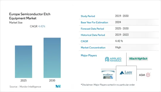
歐洲半導體蝕刻設備市場預計在預測期內複合年成長率為4.42%

主要亮點
- 歐洲半導體蝕刻設備市場依賴擴大內部半導體製造來避免全球供應鏈缺口。歐盟正在考慮在歐洲建造先進的半導體工廠,以避免依賴美國和亞洲的半導體及外圍元件供應。歐盟正在探索生產尺寸小於 10 奈米的半導體的方法,最終縮小到 2 奈米晶片。例如,歐盟宣布了針對半導體的重大補貼制度,目標是根據《歐盟晶片法案》,到2030年動員430億歐元的公共和私人投資用於半導體研究、設計和生產。
- 作為新興經濟體,該地區的 5G 無線系統、聯網汽車和高效能運算市場正在強勁成長。由於半導體的使用對於上述所有市場都至關重要,因此該地區的半導體蝕刻設備市場正在間接成長。例如,化合物半導體行業等離子體處理設備的領先供應商Samco宣佈在列支敦士登的Samco-ucp ltd安裝電漿蝕刻系統和UV臭氧清洗系統。
- 歐洲的工業自動化也正在推動歐洲半導體製造業的成長。例如,英特爾選擇德國作為大型新晶片製造基地的所在地,這是整個歐洲 880 億美元投資計劃中的首個項目,旨在減少對進口的依賴並緩解製造商的供不應求。 。
- 出於多種原因,原料和零件的來源正在轉移到歐盟之外,包括為了避免遵守 REACH(法規和授權)等嚴格的環境法規。原料加工廠和零件製造搬遷到歐盟之外,破壞了歐盟某些地區現有供應鏈的穩定。建構新的供應商生態系統增加了晶片製造商的業務支出,並增加了供應商的不確定性。此外,對該地區某些化合物的使用限制也會限制設計靈活性和創新潛力。這些都是歐洲半導體蝕刻設備市場成長的挑戰。
- COVID-19 對歐洲半導體蝕刻設備市場產生了負面影響,導致半導體產業的供應鏈和生產中斷。勞動力短缺對半導體蝕刻設備製造商的影響尤其嚴重。疫情期間,全球半導體供應鏈中的公司被迫縮減或取消營運。由於汽車等行業需要半導體,該領域出現了嚴重的虧損和需求的增加,導致該地區供應鏈出現巨大缺口。
歐洲半導體蝕刻設備市場趨勢
該市場是由政府和歐盟晶片法案戰略推動的,該戰略正在促進半導體和外圍產品的內部生產,以避免全球供應鏈缺口。
- 《歐洲晶片法案》旨在提高歐洲在半導體技術和應用方面的競爭力和彈性,並加速該地區的數位化和綠色轉型。為了實現該地區的永續成長,歐盟正在規劃發展該地區整個價值鏈的藍圖,其中包括半導體蝕刻設備製造商。該地區許多國家開始接受這項策略。例如,英國政府正在尋求業界對國內半導體產業和晶片供給能力狀況的回饋。
- 德國經濟部長宣布,德國願意向「歐洲通用利益關鍵計劃」投資 30 億歐元,這是歐盟刺激投資和減少對進口依賴的關鍵補貼工具。德國政府打算用這筆錢建造新的半導體製造工廠。這項投資的重點是減少未來半導體需求對進口的依賴。
- 大學、政府和企業正在共同努力開發該地區半導體的新蝕刻技術。例如,威爾斯政府正在資助一個由斯旺西大學主導的計劃,並與合作夥伴合作開發世界領先的半導體製程技術。應用範例包括自動駕駛汽車、新型清潔能源設備、未來移動、人工智慧、先進封裝、生物感測器和穿戴式感測器。 SPTS Technologies(KLA 公司)、IQE、化合物半導體中心 (CSC)、Biovici、BioMEMS、斯旺西大學和卡迪夫大學以及整合化合物半導體有限公司是 ASSET(專用半導體蝕刻)的少數合作夥伴。
- 該地區正在發展半導體及相關領域的內部製造。在歐洲,政府的支持措施正在增加對新興企業的資助。例如,Almi Invest 在 AlixLabs 投入了約 300 萬瑞典克朗,該公司正在研究使半導體元件更便宜、更快的新方法。瑞典隆德的 AlixLab 發明了原子層蝕刻間距分裂,這是一種用於半導體元件製造的革命性新技術,消除了製造過程中的許多步驟。
多功能先進半導體晶片在工業自動化中的應用正在推動該地區的半導體蝕刻設備市場。
- 歐洲公司正在透過跨產業引入自動化進行轉型。半導體的應用在這一自動化過程中至關重要,並且正在推動該地區的半導體蝕刻設備市場。在歐盟,產業聯盟是半導體技術和處理器領域的趨勢。
- 此次合作的目的是確定現有差距和所需的技術發展,以提高歐盟半導體產業(特別是歐洲中小企業)的公司和研發機構的競爭力。在密集型產業中,這種合作有助於組織克服進入障礙、達到臨界點並減少依賴。
- 許多全球半導體製造商都有興趣在歐洲開發高性能工業半導體。例如,英飛凌科技公司宣布將在奧地利菲拉赫的新晶片工廠開始生產,該工廠也是功率半導體能力中心。英飛凌科技公司在這裡開發了 300 毫米厚晶圓的功率半導體製造,後來在德國德勒斯登擴展到全自動化大規模生產。這種製造設備需要蝕刻設備,這將直接或間接擴大歐洲半導體蝕刻設備市場。
- 具有新興技術功能的半導體是工業自動化的組成部分。該地區大力投資生產高科技半導體製造設備。例如,德國工程技術公司博世在德勒斯登建成了一座新的半導體工廠,該工廠完全採用5G行動技術連網。博世在這座高科技設施上投資了約 10 億歐元,成為其 130 年歷史上最大的單筆投資。各種半導體蝕刻設備是製造半導體晶片不可或缺的。
歐洲半導體蝕刻設備產業概況
由於少數參與企業主導市場,半導體蝕刻設備市場趨勢已鞏固。進入這個市場需要大量資金,這為新進入者設置了障礙。主要企業正專注於產品創新、併購等策略,以確保在歐洲市場佔有較大佔有率。
- 2022 年 3 月:英特爾投資約 130 億美元改善擴建其位於愛爾蘭萊克斯利普的工廠。英特爾計劃在升級後的工廠支援Intel4製程(以前稱為7nm)。該計劃目前正在進行中,預計將於 2023 年開始生產。
- 2022 年 4 月:3M 位於比利時的半導體冷卻劑工廠無限期關閉。該工廠佔全球半導體冷卻劑產量的80%。
- 2022 年 6 月:義大利電力測試設備製造商 Colllaudi Elettronici Automatizzati 被日本 Advantest (CREA) 收購。 CREA 是一家領先的供應商,在設計和製造功率半導體測試設備方面擁有豐富的經驗。此次收購將使 Advantest 能夠為高成長產業中更廣泛的客戶提供更廣泛的測試和測量解決方案。
其他好處
- Excel 格式的市場預測 (ME) 表
- 3 個月分析師支持
目錄
第1章簡介
- 研究成果
- 研究場所
- 調查範圍
第2章調查方法
第3章執行摘要
第4章市場動態
- 市場概況
- 市場促進因素
- 政府和歐盟針對半導體及外圍產品內部生產的晶片法戰略,以避免全球供應鏈缺口
- 多功能先進半導體晶片在工業自動化的應用
- 市場限制因素
- 建構區域供應商生態系統
- 價值鏈分析
- 波特五力分析
- 新進入者的威脅
- 買家/消費者的議價能力
- 供應商的議價能力
- 替代品的威脅
- 競爭公司之間敵對關係的強度
- COVID-19 對市場的影響
第5章市場區隔
- 依產品類型
- 高密度蝕刻設備
- 低密度蝕刻設備
- 依蝕刻類型
- 導體蝕刻
- 介電蝕刻
- 多晶矽蝕刻
- 按用途
- 邏輯和記憶
- 功率元件
- MEMS
- 按國家/地區
- 英國
- 德國
- 法國
- 義大利
- 歐洲其他地區
第6章 競爭狀況
- 公司簡介
- Applied Materials Inc.
- Hitachi High Technologies America Inc.
- Lam Research Corporation
- RENA Technologies GmbH
- SPS-Europe
- ASM International
- Lattice Semiconductor Corporation
- Texas Instruments
- Trymax Semiconductor Equipment BV
第7章 投資分析
第8章市場的未來
簡介目錄
Product Code: 90902
The Europe Semiconductor Etch Equipment Market is expected to register a CAGR of 4.42% during the forecast period.

Key Highlights
- The Semiconductor Etch Equipment market in Europe is dependent on expanding the in-house semiconductor manufacturing to avoid the global supply chain gap. European Union is considering building advanced semiconductor factories in Europe to avoid relying on the U.S. and Asia to supply semiconductors and peripheral components. The EU explores how to produce semiconductors with features smaller than 10 nm and eventually down to 2 nm chips. For instance, the EU has announced a significant subsidy program for semiconductors and will contribute EURO 11 billion in public money for semiconductor research, design, and production under the EU Chips Act to mobilize EURO 43 billion in public and private investment by 2030.
- The region is witnessing high growth in 5G wireless systems, connected cars, and high-performance computing markets as a developed economy. Usage of semiconductors is essential for all the above-said markets, and thus the semiconductor etch equipment market is growing in the region indirectly. For instance, Samco, a leading provider of plasma processing equipment for the compound semiconductor industry, has announced the installation of a plasma etch system and a UV ozone cleaning system at Samco-ucp ltd in Liechtenstein.
- Industrial automation in Europe is also propelling the growth of semiconductor manufacturing in Europe. For instance, Intel has chosen Germany as the location for a massive new chipmaking complex, revealing the first details of a USD 88 billion investment drive throughout Europe to reduce reliance on imports and alleviate a supply shortage for manufacturers.
- Raw material and component providers are relocating outside the EU for various reasons, including avoiding complying with stringent environmental regulations such as REACH (restriction and authorization). Any migration of raw material processing factories and component manufacturing outside the EU destabilizes the established supply networks in a specific EU region. Creating a new supplier ecosystem increases chip makers' expenses of doing business and increases supplier uncertainty. Furthermore, the restrictions on using certain chemical compounds in the region may limit design flexibility and innovation potential. These are the challenges for the European Semiconductor Etch Equipment market to grow.
- COVID-19 has negatively influenced the European Semiconductor Etch Equipment market, causing supply chain and production disruptions in the semiconductor sector. The impact on semiconductor etch equipment manufacturers was particularly severe due to labor shortages. Companies in the semiconductor supply chain worldwide were forced to reduce or even discontinue operations during the pandemic. Because semiconductors are required for industries such as automobiles, the sector has been plagued by a significant deficit and rising demand, resulting in a massive supply chain gap in the region.
Europe Semiconductor Etch Equipment Market Trends
The Governments and EU Chips Act strategies for the manufacturing of in-house semiconductors and peripheral products to avoid the global supply chain gap is driving the market.
- The European Chips Act intends to boost Europe's competitiveness and resilience in semiconductor technologies and applications and facilitate the region's digital and green transformation. To have sustainable growth in the region, the EU has planned a blueprint to develop the whole value chain in the region, including the semiconductor etch equipment manufacturer. Many countries in the region have started working on the strategy; for instance, the government of the United Kingdom is seeking industry feedback on the condition of the domestic semiconductor industry and its ability to provide chips.
- The Economy Minister of Germany has stated that Germany is willing to invest EUR 3 billion in the initiative "Important Projects of Common European Interest," which is the EU's key subsidy tool to stimulate investment and reduce dependence on imports. The German government intends to invest the money to establish new semiconductor manufacturing plants. This investment is primarily focused on decreasing the dependency on semiconductor imports for future semiconductor needs.
- Universities, governments, and companies are working collaboratively to develop new etching technology for semiconductors in the region. For instance, The Wales Government has funded a project led by Swansea University and involves partners to create world-leading semiconductor process technology. Some of the applications are autonomous vehicles, new clean energy devices, future mobility, artificial intelligence, advanced packaging, biosensors, and wearable sensors. SPTS Technologies (a KLA company), IQE, The Compound Semiconductor Centre (CSC), Biovici, BioMEMS, Swansea and Cardiff universities, and Integrated Compound Semiconductors Ltd are among few partners in the ASSET (Application Specific Semiconductor Etching).
- In-house manufacturing of semiconductors and allied sectors are developing in the region. Start-up funding is increasing in Europe by virtue of the supporting governmental policies. For instance, Almi Invest is putting about SEK 3 million into AlixLabs, which is working on a new way of making semiconductor components that is both cheaper and faster. AlixLabs of Lund, Sweden, has invented Atomic Layer Etch Pitch splitting, a new, revolutionary technology for manufacturing semiconductor components that removes many phases in the manufacturing process.
The application of multi-functional advanced semiconductor chips in industrial Automations is driving the semiconductor Etch Equipment Market in the Region.
- Companies in the European region are transforming by implementing automation in their industries. In this automation process application of semiconductors is essential and thus drives the semiconductor etch equipment market in the region. Industrial alliances are trending in the EU for Semiconductor Technologies and Processors sectors.
- The alliance's goal is to identify existing gaps and technological developments needed to improve the competitiveness of enterprises and research and technology organizations working in the industry in the EU, particularly smaller European players. In a concentrated industry, this cooperation aids organizations in overcoming entrance obstacles, achieving critical mass, and reducing dependency.
- Many global semiconductor manufacturers are interested in developing highly functional industrial semiconductors in the European region because of the opportunity to become a complete solution provider to the companies in the region in their automation process. For example, Infineon Technologies announced that it plans to start manufacturing at its new chip plant in Villach, Austria, where it also maintains its power semiconductor competence center. The business developed power semiconductor manufacture on 300mm thin wafers here and later expanded into fully automated high-volume production in Dresden, Germany. For this manufacturing unit, etching equipment would be required, directly or indirectly increasing the European Semiconductor Etch Equipment market.
- Semiconductors with emerging technology functionality are the building blocks of Industrial Automation. The region is gearing up with huge investment in manufacturing high-tech semiconductor manufacturing units. For example, Bosch, a German engineering and technology firm, has completed a new semiconductor plant in Dresden fully networked with 5G mobile technology. Bosch had put roughly EURO 1 billion into the high-tech facility, making it the company's most significant single investment in its 130-year history. Requirement for various semiconductor etching equipment is essential for manufacturing the semiconductor chips.
Europe Semiconductor Etch Equipment Industry Overview
The trend in the semiconductor etch equipment market is consolidated owing to the presence of a few players dominating the market. The significant capital required to enter this market has become a barrier for new entrants. The key players are focusing more on product innovation, mergers, and acquisitions, among other strategies, to hold a significant market share in the Europe market.
- March 2022: Intel invests about USD 13 billion to improve and expand its fabs in Leixlip, Ireland. The chipmaker plans to accommodate Intel 4 process (previously known as 7 nm) in the upgraded plant. The project is currently underway, with output expected to begin in 2023.
- April 2022: 3M's semiconductor coolant plant in Belgium has been closed indefinitely whose products were used in semiconductor etching processes. The plant accounts for 80 percent of the global semiconductor coolant output.
- June 2022: Collaudi Elettronici Automatizzati, an Italian manufacturer of power test equipment, has been acquired by Advantest in Japan (CREA). CREA is a leading supplier of power semiconductor test equipment, having extensive experience in the design and manufacture of test equipment for power semiconductors. Advantest will be able to offer a greater range of test and measurement solutions to a broader range of customers in high-growth industries because of this acquisition.
Additional Benefits:
- The market estimate (ME) sheet in Excel format
- 3 months of analyst support
TABLE OF CONTENTS
1 INTRODUCTION
- 1.1 Study Deliverables
- 1.2 Study Assumptions
- 1.3 Scope of the Study
2 RESEARCH METHODOLOGY
3 EXECUTIVE SUMMARY
4 MARKET DYNAMICS
- 4.1 Market Overview
- 4.2 Market Drivers
- 4.2.1 The Governments and EU Chips Act strategies for the manufacturing of in-house semiconductors and peripheral products to avoid the global supply chain gap
- 4.2.2 The application of multi-functional advanced semiconductor chips in industrial Automations
- 4.3 Market Restraints
- 4.3.1 Creating an in-house supplier ecosystem in the region
- 4.4 Value Chain Analysis
- 4.5 Porter's Five Force Analysis
- 4.5.1 Threat of New Entrants
- 4.5.2 Bargaining Power of Buyers/Consumers
- 4.5.3 Bargaining Power of Suppliers
- 4.5.4 Threat of Substitute Products
- 4.5.5 Intensity of Competitive Rivalry
- 4.6 COVID-19 Impact on the Market
5 MARKET SEGMENTATION
- 5.1 By Product Type
- 5.1.1 High-density Etch Equipment
- 5.1.2 Low-density Etch Equipment
- 5.2 By Etching Type
- 5.2.1 Conductor Etching
- 5.2.2 Dielectric Etching
- 5.2.3 Polysilicon Etching
- 5.3 By Application
- 5.3.1 Logic and Memory
- 5.3.2 Power Devices
- 5.3.3 MEMS
- 5.4 By Country
- 5.4.1 United Kingdom
- 5.4.2 Germany
- 5.4.3 France
- 5.4.4 Italy
- 5.4.5 Rest of Europe
6 COMPETITIVE LANDSCAPE
- 6.1 Company Profiles
- 6.1.1 Applied Materials Inc.
- 6.1.2 Hitachi High Technologies America Inc.
- 6.1.3 Lam Research Corporation
- 6.1.4 RENA Technologies GmbH
- 6.1.5 SPS-Europe
- 6.1.6 ASM International
- 6.1.7 Lattice Semiconductor Corporation
- 6.1.8 Texas Instruments
- 6.1.9 Trymax Semiconductor Equipment BV
7 Investment Analysis
8 Future of the Market
02-2729-4219
+886-2-2729-4219


