


 |
市場調查報告書
商品編碼
1644850
高階半導體封裝:市場佔有率分析、產業趨勢與統計、成長預測(2025-2030 年)High-end Semiconductor Packaging - Market Share Analysis, Industry Trends & Statistics, Growth Forecasts (2025 - 2030) |
||||||
※ 本網頁內容可能與最新版本有所差異。詳細情況請與我們聯繫。
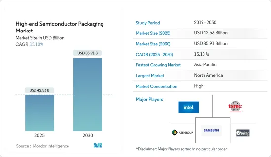
高階半導體封裝市場規模預計在 2025 年為 425.3 億美元,預計到 2030 年將達到 859.1 億美元,預測期內(2025-2030 年)的複合年成長率為 15.1%。
使用封裝來提高電子系統的性能、可靠性和成本效益,正在推動各個行業終端用戶垂直領域的需求不斷成長,而整合度、能源效率和產品特性的不斷進步則推動著市場的成長。
主要亮點
- 封裝可保護電子系統免受高頻噪音輻射、靜電放電、機械損壞和冷卻的影響。全球半導體產業的不斷成長是推動半導體封裝市場成長的主要因素之一。此外,2023年2月,半導體產業協會(SIA)宣布,2022年全球半導體產業銷售額將達到5,741億美元,創歷史最高年度總合,較上年的5,559億美元成長3.3%。
- 此外,物聯網和人工智慧的興起以及複雜電子設備的激增,正在推動家電和汽車行業的高階應用領域。這些因素正在推動更先進的半導體封裝技術來維持需求。該領域研究活動的活性化進一步推動了市場需求。
- 此外,由於 5G、物聯網、汽車和 HPC 等多個長期成長動力,半導體封裝市場預計將擴大。例如,印度政府已核准一項 100 億美元的獎勵計劃,用於建立包括晶圓廠、本土晶片設計和複合半導體工廠在內的完整的半導體生態系統。
- 此外,新冠疫情對電子產業產生了重大影響,半導體供應鏈問題和晶片短缺在一段時間內影響了該產業。然而,預計全球範圍內對半導體行業的投資增加和半導體製造設施的建立將推動後疫情時代的市場成長。
高階半導體封裝市場趨勢
消費性電子產業可望推動市場
- 消費性電子部門正大力投資半導體封裝市場。智慧型手機的成長、穿戴式裝置和智慧型裝置的日益普及以及消費性物聯網裝置在智慧家庭等應用中的不斷滲透是影響這一領域成長的一些因素。愛立信預計,2022年全球智慧型手機行動網路用戶數將達到約66億,到2028年將超過78億人。
- 此外,由於複雜的半導體元件所能提供的功能和特性越來越多,智慧型手錶和智慧揚聲器市場近年來變得極為受歡迎。因此,對Wi-Fi和藍牙晶片的需求急劇增加。家電製造商也正在利用半導體元件為其產品配備物聯網和人工智慧模型,以改善用戶體驗並使其產品更加明亮。
- 例如,華為在2023年3月宣布,計劃在未來幾年推出一款電池功能重大升級的折疊式智慧型手機。該設備具有電池升級功能。此外,華為預計將採用高矽陽極材料來增強智慧型手機的電池容量,預計將達到 5,060 mAh。
- 對於在技術上投入大量資金的年輕消費者來說,電腦和筆記型電腦已經成為必需品。此外,預計未來十年電子領域的技術創新和進步將推動半導體封裝銷售。物聯網和人工智慧的採用預計將推動全球新興市場和已開發市場的半導體封裝銷售成長。
- 英特爾公司和倫敦大學學院 (UCL) 聯手推出了一款可透過手勢和臉部手勢進行操作和控制的新型非接觸式電腦。電子市場不斷追求更高的功耗、更快的速度、更高的引腳數、更小的佔用空間和更薄的外形。半導體的小型化和整合化使得智慧型手機、平板電腦和新興的物聯網設備等消費性電子產品變得更輕、更小、更便攜。
北美:市場正在經歷顯著成長
- 美國和加拿大的半導體產業在未來的關鍵技術中佔據重要地位,包括人工智慧、量子運算和 5G 等先進無線網路。
- 例如,根據GSMA的預測,到2025年,5G將成為美國領先的網路技術。 5G 網路的不斷部署與對更即時、高效能運算設備的需求不斷成長相吻合,而半導體是其中的關鍵要素。
- 美國政府正大力投資推動先進技術的應用,從而增強對高階半導體封裝的需求。美國參議院提出《促進美國製造半導體(FABS)法案》。該法案可能為半導體製造設備和工廠的投資提供25%的投資稅額扣抵。
- 此外,美國是最大的電動車市場之一,近年來電動車銷量快速成長。根據汽車創新聯盟的數據,2023 年第四季該國的電動車銷量將超過 377,000 輛,較 2022 年第四季成長 34%。
- 近年來,日本推出了多項法規以推廣電動車的使用。例如,紐約州立法機構通過了一項法案,要求到 2035 年該州銷售的所有新乘用車都必須是電動車。此外,美國也設定了2030年國內銷售的汽車中有一半是電動車的目標。
高階半導體封裝產業概況
高階半導體封裝市場正在整合。公司正在利用產品創新、擴張和夥伴關係來保持競爭優勢並擴大其市場範圍。
- 2024 年 5 月著名半導體封裝測試公司矽品精密工業 (SPIL) 最近在檳城 Bandar Cassia 科技園區開設了馬來西亞 P1 工廠。未來15年,矽品計畫推出包括晶圓凸塊加工在內的新技術,並提供包括晶圓凸塊加工、晶圓級晶片封裝、覆晶構裝和測試在內的完整承包解決方案。
- 2024 年 3 月韓國 Nepes 公司與西門子 EDA 合作,解決先進 3D-IC 封裝中複雜的熱、機械和IC封裝設計挑戰。 Nepes 專注於晶圓級、扇出型晶圓級和麵板級封裝設計。 Nepes 正在利用其專業知識透過西門子 EDA 技術(包括 Calibre nmPlatform、HyperLynx 和 Xpedition 軟體)來推動封裝創新。透過整合這些西門子解決方案,Nepes 增強了其設計能力,使其能夠為全球 IC 客戶提供 2.5D/3D 晶片設計的快速可靠服務。
其他福利
- Excel 格式的市場預測 (ME) 表
- 3 個月的分析師支持
目錄
第 1 章 簡介
- 研究假設和市場定義
- 研究範圍
第2章調查方法
第3章執行摘要
第4章 市場洞察
- 市場概況
- 產業吸引力-波特五力分析
- 供應商的議價能力
- 買家的議價能力
- 新進入者的威脅
- 替代品的威脅
- 競爭對手之間的競爭強度
- 產業價值鏈分析
- 評估宏觀經濟趨勢對市場的影響
第5章 市場動態
- 市場促進因素
- 各行業對半導體裝置的消費不斷增加
- 擴大 3D 列印在半導體封裝的應用
- 市場限制
- 半導體IC設計初期投入高,複雜度增加
第6章 市場細分
- 依技術分類
- 3D SoC
- 3D堆疊內存
- 2.5D 中介層
- UHD FO
- 內建 Si 橋
- 按最終用戶
- 消費性電子產品
- 航太和國防
- 醫療設備
- 電訊
- 車
- 其他最終用戶
- 按地區
- 北美洲
- 美國
- 加拿大
- 歐洲
- 英國
- 德國
- 法國
- 義大利
- 亞洲
- 中國
- 印度
- 日本
- 澳洲和紐西蘭
- 東南亞
- 拉丁美洲
- 中東和非洲
- 北美洲
第7章 競爭格局
- 公司簡介
- Intel Corporation
- Taiwan Semiconductor Manufacturing Company
- Advanced Semiconductor Engineering Inc.
- Samsung Electronics Co. Ltd
- Amkor Technology Inc.
- JCET Group Co. Ltd
- TongFu Microelectronics Co. Ltd
- Fujitsu Limited
- Siliconware Precision Industries Co. Ltd
- Powertech Technology Inc.
第8章投資分析
第9章:市場的未來
The High-end Semiconductor Packaging Market size is estimated at USD 42.53 billion in 2025, and is expected to reach USD 85.91 billion by 2030, at a CAGR of 15.1% during the forecast period (2025-2030).
The continuous advancements in integration, energy efficiency, and product characteristics because of the growing demand across various end-user verticals of the industry and the use of packaging for improving the performance, reliability, and cost-effectiveness of electronic systems accelerate the market's growth.
Key Highlights
- Packaging protects an electronic system from radio frequency noise emission, electrostatic discharge, mechanical damage, and cooling. The rise in the semiconductor industry worldwide is one of the major factors driving the growth of the semiconductor packaging market. In addition, in February 2023, the Semiconductor Industry Association (SIA) announced global semiconductor industry sales totaled USD 574.1 billion in 2022, the highest-ever annual total and an increase of 3.3% compared to the previous year's total of USD 555.9 billion.
- Furthermore, the rise of IoT and AI and the proliferation of complex electronics drive the high-end application segment in the consumer electronics and automotive industries. Due to these factors, more advanced semiconductor packaging technologies are being adopted to sustain demand. The growing research activities in the sector further bolstered the market's demand.
- Furthermore, the semiconductor packaging market is expected to expand due to multiple long-term growth drivers, like 5G, IoT, automotive, and HPC. For instance, the Government of India approved a USD 10 billion incentive package to build a complete semiconductor ecosystem, including fabs, home-grown chip design, and compound semiconductor plants.
- Moreover, the COVID-19 pandemic significantly impacted the electronics industry, with semiconductor supply chain issues and the chip shortage affecting the industry for some time. However, the growing investments in the semiconductor industry and increased establishments of semiconductor manufacturing facilities worldwide are anticipated to propel the market's growth in the post-pandemic era.
High-end Semiconductor Packaging Market Trends
Consumer Electronics Sector is Expected to Boost the Market
- The consumer electronics sector is significantly investing in the semiconductor packaging market. Growth of the smartphone, rising wearable and smart device adoption, and increasing consumer IoT device penetration in applications like smart homes are a few of the influential factors influencing the segment's growth. According to Ericsson, smartphone mobile network subscriptions worldwide reached nearly 6.6 billion in 2022, and they are predicted to exceed 7.8 billion by 2028.
- Additionally, markets for smartwatches and smart speakers have become extremely popular in recent years due to the growing number of features and functionalities they can offer due to sophisticated semiconductor components. As a result, the demand for Wi-Fi and Bluetooth chips increased dramatically. Consumer electronics manufacturers also use semiconductor components to equip their products with IoT and AI models, enhancing user experience and making products brighter.
- For instance, in March 2023, Huawei planned to launch its foldable smartphone with a significant battery upgrade in the coming years. The device will feature an upgrade to its battery. Further, Huawei is expected to use a high-silicon anode material to enhance the smartphone's battery capacity, which is expected to be 5,060 mAh.
- Personal computers and laptops are now essential for young consumers who are heavily invested in technology. In addition, over the next ten years, innovation and advancement in the electronics sector are anticipated to drive semiconductor packaging sales. Sales of semiconductor packaging are expected to increase globally in both developing and developed markets due to the introduction of IoT and AI.
- Intel Corporation and the University College London (UCL) have collaborated to introduce a new touchless computer that can be operated and controlled by gesturing the hands and face. Higher power dissipation, faster speeds, higher pin counts, smaller footprints, and lower profiles are all constant demands in the electronics market. Semiconductor miniaturization and integration have resulted in lighter, smaller, and more portable appliances such as smartphones, tablets, and emerging IoT devices.
North America to Experience Significant Market Growth
- The semiconductor sector in the United States and Canada has maintained a significant position in key future technologies, such as AI, quantum computing, and sophisticated wireless networks like 5G.
- For instance, as per GSMA, 5G will become the lead network technology in the United States by 2025. The increasing implementation of 5G networks coincides with the growing demand for more immediate high-performance computing appliances, for which semiconductors form a critical element.
- The US government has significantly invested in boosting the penetration of advanced technologies, bolstering the demand for high-end semiconductor packaging. The US Senate announced the Facilitating American-Built Semiconductors (FABS) Act, which may provide tax incentives to semiconductor manufacturers. The bill may establish a 25% investment tax credit for semiconductor manufacturing investments in equipment or fabs.
- Furthermore, the United States is one of the largest markets for electric vehicles, and the country has also recorded rapid growth in EV sales in recent years. More than 377,000 EVs were sold in the country in Q4 2023, registering a 34% increase from Q4 2022, according to Alliance for Automotive Innovation.
- Many regulations have been implemented in recent years to promote the use of electric vehicles in the country. For instance, New York state lawmakers passed a bill that essentially mandates that all new passenger cars sold in the state run on electric power by 2035. Moreover, the United States has set a target to ensure half of the vehicles sold in the country are electric by 2030.
High-end Semiconductor Packaging Industry Overview
The high-end semiconductor packaging market is consolidated. Companies employ product innovation, expansions, and partnerships to stay ahead of the competition and widen their market reach.
- May 2024: Siliconware Precision Industries Co. Ltd (SPIL), a prominent player in semiconductor packaging and testing, recently marked the commencement of its Malaysia P1 plant at Bandar Cassia Technology Park, Pulau Pinang. Over the next 15 years, SPIL plans to roll out new technologies, including wafer bumping, and provide a holistic turnkey solution encompassing wafer bumping, wafer-level chip packaging, flip chip packaging, and testing.
- March 2024: Nepes Corporation in South Korea partnered with Siemens EDA to address complex thermal, mechanical, and IC packaging design challenges in advanced 3D-IC packages. Nepes specializes in wafer-level, fan-out wafer-level, and panel-level packaging designs. Expanding on its expertise, Nepes is driving packaging innovations using Siemens EDA's technologies, including the Calibre nmPlatform, HyperLynx, and Xpedition software. By integrating these Siemens solutions, Nepes has enhanced its design capabilities, enabling swift and dependable services in 2.5D/3D chiplet designs for its global IC clientele.
Additional Benefits:
- The market estimate (ME) sheet in Excel format
- 3 months of analyst support
TABLE OF CONTENTS
1 INTRODUCTION
- 1.1 Study Assumptions and Market Definitions
- 1.2 Scope of the Study
2 RESEARCH METHODOLOGY
3 EXECUTIVE SUMMARY
4 MARKET INSIGHTS
- 4.1 Market Overview
- 4.2 Industry Attractiveness - Porter's Five Forces Analysis
- 4.2.1 Bargaining Power of Suppliers
- 4.2.2 Bargaining Power of Buyers
- 4.2.3 Threat of New Entrants
- 4.2.4 Threat of Substitute Products
- 4.2.5 Intensity of Competitive Rivalry
- 4.3 Industry Value Chain Analysis
- 4.4 Assessment of the Impact of Macroeconomic Trends on the Market
5 MARKET DYNAMICS
- 5.1 Market Drivers
- 5.1.1 Growing Consumption of Semiconductor Devices Across Industries
- 5.1.2 Growing Adoption of 3D Printing in Semiconductor Packaging
- 5.2 Market Restraints
- 5.2.1 High Initial Investment and Increasing Complexity of Semiconductor IC Designs
6 MARKET SEGMENTATION
- 6.1 By Technology
- 6.1.1 3D SoC
- 6.1.2 3D Stacked Memory
- 6.1.3 2.5D interposers
- 6.1.4 UHD FO
- 6.1.5 Embedded Si Bridge
- 6.2 By End User
- 6.2.1 Consumer Electronics
- 6.2.2 Aerospace and Defense
- 6.2.3 Medical Devices
- 6.2.4 Telecom and Communication
- 6.2.5 Automotive
- 6.2.6 Other End Users
- 6.3 By Geography
- 6.3.1 North America
- 6.3.1.1 United States
- 6.3.1.2 Canada
- 6.3.2 Europe
- 6.3.2.1 United Kingdom
- 6.3.2.2 Germany
- 6.3.2.3 France
- 6.3.2.4 Italy
- 6.3.3 Asia
- 6.3.3.1 China
- 6.3.3.2 India
- 6.3.3.3 Japan
- 6.3.3.4 Australia and New Zealand
- 6.3.3.5 South East Asia
- 6.3.4 Latin America
- 6.3.5 Middle East and Africa
- 6.3.1 North America
7 COMPETITIVE LANDSCAPE
- 7.1 Company Profiles
- 7.1.1 Intel Corporation
- 7.1.2 Taiwan Semiconductor Manufacturing Company
- 7.1.3 Advanced Semiconductor Engineering Inc.
- 7.1.4 Samsung Electronics Co. Ltd
- 7.1.5 Amkor Technology Inc.
- 7.1.6 JCET Group Co. Ltd
- 7.1.7 TongFu Microelectronics Co. Ltd
- 7.1.8 Fujitsu Limited
- 7.1.9 Siliconware Precision Industries Co. Ltd
- 7.1.10 Powertech Technology Inc.
8 INVESTMENTS ANALYSIS
9 FUTURE OF THE MARKET
 2025 年至 2033 年半導體封裝市場規模、佔有率、趨勢及預測(按類型、封裝材料、技術、最終用戶和地區)
 半導體封裝:市場佔有率分析、產業趨勢與統計、成長預測(2025-2030 年)
 3-D TSV:關鍵問題洞察與市場分析
 高密度封裝(MCM、MCP、SIP、3D-TSV):市場分析與技術趨勢
 2025 年 3D 半導體封裝全球市場報告
 先進半導體封裝市場:未來預測(2025-2030)
 半導體封裝市場規模、佔有率和成長分析(按材料、封裝技術、最終用途行業和地區)- 2025-2032 年行業預測
 全球 MEMS 封裝 -市場佔有率分析、產業趨勢/統計、成長預測(2025-2030 年)
 半導體仿真器的全球市場:2024年
 半導體先進封裝市場 2025-2029