


 |
市場調查報告書
商品編碼
1651039
3D TSV 和 2.5D -市場佔有率分析、行業趨勢和統計、成長預測(2025-2030 年)3D TSV And 2.5D - Market Share Analysis, Industry Trends & Statistics, Growth Forecasts (2025 - 2030) |
||||||
※ 本網頁內容可能與最新版本有所差異。詳細情況請與我們聯繫。
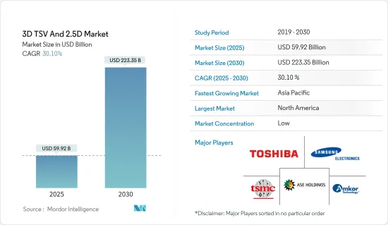
3D TSV 和 2.5D 市場規模在 2025 年預計為 599.2 億美元,預計到 2030 年將達到 2233.5 億美元,預測期內(2025-2030 年)的複合年成長率為 30.1%。
半導體產業的封裝正在經歷持續的變革。隨著半導體應用的成長,CMOS 擴展放緩和價格上漲迫使該行業依賴IC封裝的進步。 3D增材技術是滿足AI、ML和資料中心等應用效能要求的解決方案。因此,在預測期內,對高效能運算應用的不斷成長的需求主要推動了矽通孔 (TSV) 市場的發展。
關鍵亮點
- 3D TSV 封裝技術也越來越受到重視。與目前的焊線技術相比,晶片之間的資料傳輸時間減少,從而提高速度並顯著降低功耗。 2022年10月,台積電宣布推出開箱即用的3DFabric聯盟。這是台積電開放創新平台(OIP)的介紹,該平台可協助客戶克服快速成長的半導體和系統級設計挑戰。它還將有助於加速下一代 HPC 和行動技術進步與台積電 3DFabric 技術的融合。
- 消費者對電子設備的需求不斷成長,引發了對先進半導體設備的需求,以實現各種新功能。隨著對半導體設備的需求不斷成長,先進的封裝技術正在提供當今數位化世界所需的外形規格和處理能力。例如,根據半導體產業協會的數據,2022年8月全球半導體產業銷售額為474億美元,總合2021年8月的473億美元小幅成長0.1%。
- 而根據 GSM 協會的預測,到 2025 年,美國將成為全球智慧型手機普及率最高的國家(佔連線的 49%)。根據美國物聯網協會的數據,美國是每個家庭智慧家庭設備擁有率最高的國家,消費者擁有涵蓋兩到三個使用案例(能源、安全和家用電子電器)的家用電子電器產品的趨勢最為明顯。
- 此外,2022年9月,拜登政府宣布將投資500億美元發展國內半導體產業,以抵銷對中國的依賴,因為美國生產了零,卻消費量了全球25%對國家安全至關重要的最先進晶片。總統拜登於 2022 年 8 月簽署了價值 2800 億美元的《CHIPS 法案》,以促進國內高科技製造業的發展,這是加強美國與中國競爭的一部分。預計半導體領域的如此強勁投資將為研究市場的成長提供有利機會。
- MEMS 和感測器的成長是由汽車和工業自動化等各種應用對感測器和顯示器的需求快速成長所推動的。 2022年8月,MEMS製造商、全球半導體產業主要參與企業意法半導體(STMicroelectronics)宣布推出其第三代MEMS感測器,專為消費智慧工業、行動裝置、醫療和零售領域設計。強大的晶片大小的運動和環境感測器使當今採用 MEMS 技術構建的智慧型手機和穿戴式裝置能夠實現方便用戶使用的情境察覺功能。 ST 的最新一代 MEMS 感測器突破了輸出精度和功耗的技術極限,將性能提升到了新的水平。
- 此外,製造 TSV 設備的高成本限制了市場的成長。這不僅包括設備的成本,還包括設備正常運作所需的任何配件和消耗品的成本。此外,製造 TSV 設備的嚴格準則和規定也會推高成本。
- 此外,全球半導體短缺促使參與企業專注於疫情後擴大生產能力。例如,中芯國際已宣布了積極的計劃,將在各個城市建設自己的晶片製造廠,到2025年將產能翻倍。此外,許多亞太地方政府正在透過長期計劃資助半導體產業,預計這將有助於恢復市場成長。例如,中國政府已引入約230至300億美元資助國家積體電路投資基金2030的第二階段。
- 此外,俄羅斯和烏克蘭之間持續的衝突預計將對電子產業產生重大影響。這場衝突已經加劇了影響該行業一段時間的半導體供應鏈問題和晶片短缺問題。這種中斷可能表現為鎳、鈀、銅、鈦、鋁和鐵礦石等主要原料的價格波動,並可能導致材料短缺。這導致3D堆疊記憶體的生產受到阻礙。
3D TSV 和 2.5D 市場趨勢
LED構裝可望大幅成長
- LED 在產品中的使用日益增多,推動了高功率、更高密度、更低成本設備的擴張。與2D封裝不同,採用矽穿孔電極(TSV) 技術的3D(3D) 封裝可實現高密度垂直互連。
- TSV積體電路提供更短的連接長度,從而降低寄生電容、電感和電阻,從而實現單晶片和多功能整合的有效組合,並實現高速、低功耗互連。根據IEA預測,2025年LED在國際照明市場的滲透率預計將達到76%左右,2030年將進一步達到87.4%。
- 此外,政府採用節能 LED 的措施和法規也在推動所研究市場的發展。根據國際能源總署(IEA)的預測,到2025年,LED在照明市場的佔有率預計將成長75.8%。
- LED構裝要求還有待提高。如果LED晶片在封裝中的位置不準確,可能會直接影響整個封裝設備的發光效率。如果沒有對準,LED光就不會從反光杯中充分反射,進而影響LED的亮度。
- 美國能源局最近宣布將投資 6,100 萬美元用於 10 個試點計劃,利用最新技術將數千個家庭和企業轉變為先進的節能網路。這也適用於從白熾燈或鹵素燈泡轉換為更節能的 LED 照明。因此,隨著 LED 的擴張,預測期內美國的LED構裝需求將會成長。
- 此外,市場中的各種參與企業正在研究的市場中開發新產品。 2022 年 5 月,Lumileds LLC 推出高功率 CSP(晶片級封裝)LED。 LUXEON HL1Z 是一種非圓頂型單面光源,可在僅 1.4 平方毫米的小盒子中提供高發光效率(137lm/W 或更高)。
- LED構裝應用的快速進步預計將在未來幾年推動技術創新和消費,從而推動研究市場的成長。另一方面,高飽和度可能會限制產品的接受度,從而限制市場成長。
亞太地區可望佔據主要市場佔有率
- 亞太地區是該市場的一個重要的成長地區。智慧型手機普及率的不斷上升使得該地區成為全球領先的行動市場之一。
- 根據GSM協會統計,智慧型手機寬頻網路覆蓋亞太地區96%的人口,共有12億人使用行動網路服務。 5G 發展勢頭在亞洲持續,目前已有 14 個市場供應商使用 5G 服務。預計印度和越南等其他幾個市場也將在未來幾年內推出商業服務。到 2025 年,預計該全部區域將擁有 4 億個 5G 連接,佔總人口的 14% 以上。此外,工業4.0也是亞太地區最熱門的趨勢之一。物聯網設備和小型化是利用 3D TSV 的工業 4.0 的主要趨勢。該地區正在大力投資物聯網以支援智慧城市基礎設施。
- 科技的發展推動了家用電子電器、通訊、醫療設備、通訊設備和汽車的進步。中國即將推出 5G 服務,將刺激需求,尤其是對智慧型手機的需求。
- 據工信部稱,中國計劃在2022年安裝200萬個5G基地台,以發展下一代行動網路。根據工信部統計,目前,中國當地已建成142.5萬個5G基地台,支撐全國5億多5G用戶,是全球最完善的網路。該地區 5G 的日益普及預計將推動對 5G 設備的需求,從而增加對 2.5D 和 3D 半導體封裝的需求。
- 此外,根據中國信通院統計,5G智慧型手機出貨量佔國內出貨量的75.9%,高於全球平均的40.7%。到2022年7月,預計5G智慧型手機將佔中國行動電話整體出貨量的74%。截至2022年7月,5G行動電話總出貨量約在1.24億支部左右,中國將推出121款新5G行動電話。這些趨勢預計將加速該地區對 2.5D 和 3D 半導體封裝解決方案的需求。
- 自動駕駛汽車和電動車的使用日益增多也增加了全部區域先進半導體的需求,進一步推動了研究市場的成長。 2022年2月,特斯拉計劃在中國建造第二家電動車工廠,以滿足國內和出口市場日益成長的需求。短期內,特斯拉打算將在中國的生產能力提升至至少每年100萬輛,並計畫在上海臨港自貿區目前的展覽中心附近建立第二家工廠。此外,中國政府的目標是到2025年將電動車佔汽車總銷量的20%,其中包括採用新能源汽車作為下一代公務車。
- 此外,對半導體製造和封裝工廠的投資增加也為所研究的市場創造了有利的成長前景。例如,領先的半導體晶片製造商英特爾最近宣布將投資70億美元在馬來西亞建造先進的晶片封裝工廠。同樣,2022年11月,日月光(ASE)宣布投資3億美元擴建其在馬來西亞的生產基地。
3D TSV 和 2.5D 產業概覽
3D TSV 和 2.5D 市場競爭激烈且多樣化,擁有多種主要參與者。市場上有小型、大型和本地供應商,形成了良好的競爭。這些公司正在建立策略合作關係,以擴大市場佔有率並提高盈利。此外,該市場中的公司正在收購致力於企業網路設備技術的新興企業,以增強其產品能力。
2022 年 8 月,英特爾公佈了獨特的架構和封裝突破,有助於基於 2.5D 和 3D 的晶片設計,開創了晶片製造技術及其重要性的非凡時代。英特爾System Foundry模式的顯著特點就是增強封裝。該組織計劃在2030年將封裝電晶體的數量從1000億個提高到1兆個。
2022 年 3 月,Apple 採用 2.5D 方法為其最新的 M1 Ultra 設備提供動力,為未來利用小晶片的設計打開了大門。這種名為 UltraFusion 的封裝架構將兩個 M1 Max 晶片晶粒在矽內插器上互連,從而形成一個包含 1,140 億個電晶體的系統單晶片 (SoC)。它利用矽基基板和內插器來支援兩個具有 10,000 個低延遲互連的晶粒,並且兩個晶粒之間的處理器間頻寬為 2.5TB/s。它還連接到以 800GB/s 介面運行的 128GB 低延遲統一記憶體。
其他福利
- Excel 格式的市場預測 (ME) 表
- 3 個月的分析師支持
目錄
第 1 章 簡介
- 研究假設和市場定義
- 研究範圍
第2章調查方法
第3章執行摘要
第4章 市場洞察
- 市場概況
- 產業吸引力-波特五力分析
- 供應商的議價能力
- 買家的議價能力
- 新進入者的威脅
- 替代品的威脅
- 競爭對手之間的競爭強度
- 產業價值鏈分析
- 宏觀經濟趨勢對市場的影響
第5章 市場動態
- 市場促進因素
- 高效能運算應用市場的擴大
- 資料中心和儲存設備的成長
- 市場問題
- IC封裝單價高
第6章 技術簡介
第7章 市場區隔
- 按包裝類型
- 3D堆疊內存
- 2.5D內插器
- 帶有 TSV 的 CIS
- 3D SoC
- 其他封裝類型(LED、MEMS 和感測器等)
- 按最終用戶應用
- 消費性電子產品
- 車
- 高效能運算 (HPC) 和網路
- 其他最終用戶應用程式
- 按地區
- 北美洲
- 美國
- 加拿大
- 歐洲
- 英國
- 德國
- 法國
- 義大利
- 歐洲其他地區
- 亞太地區
- 中國
- 印度
- 日本
- 澳洲
- 東南亞
- 其他亞太地區
- 其他
- 北美洲
第8章 競爭格局
- 公司簡介
- Toshiba Corp.
- Samsung Electronics Co. Ltd.
- ASE Group
- Taiwan Semiconductor Manufacturing Company Limited
- Amkor Technology, Inc.
- Pure Storage Inc.
- United Microelectronics Corp.
- STMicroelectronics NV
- Broadcom Ltd.
- Intel Corporation
- Jiangsu Changing Electronics Technology Co. Ltd.
第9章投資分析
第10章:市場的未來
The 3D TSV And 2.5D Market size is estimated at USD 59.92 billion in 2025, and is expected to reach USD 223.35 billion by 2030, at a CAGR of 30.1% during the forecast period (2025-2030).
Packaging in the semiconductor industry has noticed a continuous transformation. As the semiconductor applications are growing, the slowdown in CMOS scaling and escalating prices have forced the industry to rely on the advancement in IC packaging. 3D stacking technologies are the solution that meets the required performance of applications like AI, ML, and data centers. Therefore, the growing requirement for high-performance computing applications mainly drives the TSV (Through Silicon Via) market over the forecast period.
Key Highlights
- The 3D TSV packaging technology is also achieving traction. It reduces data transmission time between chips and the current wire bonding technology, resulting in significantly lower power consumption with faster speed. In October 2022, TSMC announced the launch of the creative 3DFabric Alliance, a considerable introduction to TSMC's Open Innovation Platform (OIP) to help customers overcome the surging hurdles of semiconductor and system-level design challenges. It will also help in gaining rapid integration of advancements for next-generation HPC and mobile technologies using TSMC's 3DFabric technologies.
- Increasing consumer demand for electronics has sparked the need for advanced semiconductor devices that enable various new capabilities. As the demands for semiconductor appliances intensify consistently, advanced packaging techniques deliver the form factor and processing power required for today's digitized world. For instance, according to the Semiconductor Industry Association, during August 2022, global semiconductor industry sales were USD 47.4 billion, a slight boost of 0.1% over the August 2021 total of USD 47.3 billion.
- In addition, according to the GSM Association, by 2025, the United States is expected to have the highest smartphone adoption globally (49% of connections). As per the United States IoT Association, it has the highest smart home device ratio per household and the most significant consumer tendency to own appliances across two or three use cases (energy, security, and appliances).
- Moreover, in September 2022, the Biden administration announced that it would invest USD 50 billion in building up the domestic semiconductor industry to counter dependency on China, as the US produces zero and consumes 25% of the world's leading-edge chips vital for its national security. President Joe Biden signed a USD 280 billion CHIPS bill in August 2022 to boost domestic high-tech manufacturing, part of his administration's push to increase US competitiveness over China. Such robust investments in the semiconductor sector would present lucrative opportunities for the growth of the studied market.
- The growth of MEMS and Sensors is attributed to the rapidly increasing demand for sensors and displays in various applications such as automotive, industrial automation, and many others. In August 2022, STMicroelectronics, a maker of MEMS and a significant player in the worldwide semiconductor industry, launched its third generation of MEMS sensors designed for consumer smart industries, mobile devices, healthcare, and retail sectors. The robust, chip-sized motion and environmental sensors power the user-friendly, context-aware features of today's smartphones, and wearables are made on MEMS technology. ST's most recent MEMS sensor generation drives technical boundaries regarding output accuracy and power consumption, elevating performance to a new level.
- Furthermore, the high costs associated with TSV device manufacturing restrict market growth. This includes not only the cost of devices but also the cost of accessories and consumables needed for their proper functioning. Moreover, the stringent guidelines and regulations governing TSV device manufacturing also add to the charges.
- Furthermore, the worldwide semiconductor shortage encouraged players to focus on expanding production capacity during a post-pandemic. For instance, the SMIC announced aggressive plans to double its production capacity by 2025 by constructing unique chip fabrication plants in different cities. Also, many Asian-Pacific local governments have funded the semiconductor industry in a long-term program, hence anticipated to regain market growth. For instance, the Chinese government introduced roughly USD 23-30 billion to pay for the second stage of its National IC Investment Fund 2030.
- Moreover, the ongoing conflict between Russia and Ukraine is expected to impact the electronics industry significantly. The conflict has already exacerbated the semiconductor supply chain issues and the chip shortage that have affected the industry for some time. The disruption may come in the form of volatile pricing for critical raw materials such as nickel, palladium, copper, titanium, aluminum, and iron ore, resulting in material shortages. This would obstruct the manufacturing of 3D Stacked Memory.
3D TSV And 2.5D Market Trends
LED Packaging Expected to Witness the Significant Growth
- The increasing use of LED in products has promoted the expansion of higher power, greater density, and lower-cost devices. Using three-dimensional (3D) packaging through silicon via (TSV) technology authorizes a high density of vertical interconnects, unlike 2D packaging.
- TSV integrated circuits reduce connection lengths; thus, smaller parasitic capacitance, inductance, and resistance are required where a combination of monolithic and multifunctional integration is done efficiently, providing high-speed, low-power interconnects. According to IEA, the penetration rate of LEDs into the international lighting market is expected to reach some 76% in 2025 and further to 87.4% in 2030.
- Further, government initiatives and rules to adopt energy-efficient LEDs drive the studied Market. According to the International Energy Agency (IEA), the growth rate of LEDs in the lighting market is anticipated to be 75.8% in 2025.
- The requirements for LED packaging could be much better. If LED chips are not positioned into the package precisely, the luminescence efficiency of the overall packaging appliance might be affected directly. Any deviation from the established position will prevent LED light from being fully reflected from the reflective cup, affecting the LED's brightness.
- The US Department of Energy recently announced investing USD 61 million in 10 pilot projects using the latest technologies to turn thousands of homes and businesses into cutting-edge, energy-efficient networks. This applies to switching out incandescent and halogen bulbs for better energy-efficient LED lighting. As a result, with the expansion in LEDs, the LED packaging need in the United States will grow in the forecasted period.
- Furthermore, various players in the market are developing new products in the studied Market. In May 2022, Lumileds LLC launched high-power CSP (chip-scale package) LED. The LUXEON HL1Z is an un-domed, single-sided emitter that delivers high luminous efficacy (137lm/W or more) from a tiny box, just 1.4mm square.
- Rapid advancements in LED package applications are projected to raise innovation and consumption in the coming years, propelling the studied market growth. On the other hand, high saturation may limit product acceptance, which, in turn, limits market growth.
Asia-Pacific is Expected to Hold the Significant Market Share
- Asia-Pacific is the significant-growing region in the Market studied. The rising smartphone adoption rates have made the region one of the major mobile markets in the world, primarily due to the increasing population evolution and urbanization.
- As per the GSM Association, smartphone broadband networks cover 96% of the population of APAC, with 1.2 billion people accessing mobile internet services. 5G momentum continues revving across the region, with commercial 5G services currently available across 14 markets. Several others, including India and Vietnam, are expected to board in the coming years. By 2025, there will be 400 million 5G connections across the region, over 14% of the population. Further, industry 4.0 is also one of Asia-Pacific's most emerging trends. IoT devices and miniaturization are important trends in Industry 4.0, utilizing 3D TSV. The region is investing heavily in IoT to support smart city infrastructure.
- Advancing technologies have contributed to the development of consumer electronics, telecom, medical devices, communication devices, and automotive. With the launch of 5G benefits in the country, the demand for smartphones, among other things, has been rising.
- According to the MIIT, China desired 2 million installed 5G base stations in 2022 to develop the country's next-generation mobile network. The Chinese mainland presently has 1.425 million installed 5G base stations that support more than 500 million 5G users nationally, making it the most comprehensive network in the world, as per MIIT. The growing implementation of 5G in the region is also expected to promote the demand for 5G-enabled devices, thereby increasing the need for 2.5D and 3D semiconductor packaging.
- Further, according to CAICT, 5G smartphone shipments are recorded for 75.9% of domestic shipments, more significant than a global average of 40.7%. By July 2022, 5G smartphones will have reached 74% of all cellphone shipments in China. The total number of 5G cell phone shipments by July 2022 was 124mm units, and China introduced 121 latest 5G mobile phone models. Such trends would accelerate the region's demand for 2.5D and 3D semiconductor packaging solutions.
- The increasing use of autonomous and electric vehicles has also increased the demand for advanced semiconductors across the region, further supporting the studied Market's growth. In February 2022, Tesla plans to build a 2nd EV facility in China to keep up with rising demand locally and in export markets. In the short term, Tesla intends to increase capacity in China to at least 1mm cars yearly, with a second plant planned around its present exhibition in Shanghai's Lingang free trade zone. In addition, the Chinese government seeks 20% of all vehicle sales to be electric by 2025, including adopting NEVs as the next generation of government vehicles.
- Moreover, the growing investments in semiconductor manufacturing and packaging plants also create a favorable growth scenario for the studied Market. For instance, Intel, a significant semiconductor chip manufacturer, recently announced a USD 7 billion investment to build an advanced chip packaging facility in Malaysia. Similarly, in November 2022, Advanced Semiconductor Engineering (ASE) announced a USD 300 million investment to expand its production site in Malaysia.
3D TSV And 2.5D Industry Overview
The 3D TSV and 2.5D market is highly competitive and consists of various significant performers as it is diversified. The existence of small, large, and local vendors in the Market creates excellent competition. These firms leverage strategic collaborative endeavors to expand their market share and increase profitability. The companies in the Market are also acquiring start-ups performing on enterprise network equipment technologies to strengthen their product capabilities.
In August 2022, Intel showcased the unique architectural and packaging breakthroughs that help 2.5D and 3D-based chip designs, ushering in a remarkable era in chipmaking technologies and their importance. Intel's system foundry model features enhanced packaging. The organization intends to improve the number of transistors on a package from 100 billion to 1 trillion by 2030.
In March 2022, Apple adopted a 2.5D approach to boost the enactment of its latest M1 Ultra device that unlocks the door to future designs utilizing chiplets. A packaging architecture called UltraFusion interconnects the die of two M1 Max chips on a silicon interposer to build a system on a chip (SoC) with 114bn transistors. This utilizes a silicon substrate and interposer that supports the two dies with 10,000 interconnects with 2.5 TB/s of low latency and inter-processor bandwidth between the die. This also connects the die to 128 GB of low-latency unified memory operating an 800 GB/s interface.
Additional Benefits:
- The market estimate (ME) sheet in Excel format
- 3 months of analyst support
TABLE OF CONTENTS
1 INTRODUCTION
- 1.1 Study Assumptions and Market Definitions
- 1.2 Scope of the Study
2 RESEARCH METHODOLOGY
3 EXECUTIVE SUMMARY
4 MARKET INSIGHTS
- 4.1 Market Overview
- 4.2 Industry Attractiveness - Porter's Five Forces Analysis
- 4.2.1 Bargaining Power of Suppliers
- 4.2.2 Bargaining Power of Buyers
- 4.2.3 Threat of New Entrants
- 4.2.4 Threat of Substitute Products
- 4.2.5 Intensity of Competitive Rivalry
- 4.3 Industry Value Chain Analysis
- 4.4 Impact of Macroeconomic Trends on the Market
5 MARKET DYNAMICS
- 5.1 Market Drivers
- 5.1.1 Expanding Market for High Performance Computing Application
- 5.1.2 Expanding Scope of Data Centers and Memory Devices
- 5.2 Market Challenges
- 5.2.1 High Unit Cost of IC Packages
6 TECHNOLOGICAL SNAPSHOT
7 MARKET SEGMENTATION
- 7.1 By Packaging Type
- 7.1.1 3D Stacked Memory
- 7.1.2 2.5D Interposer
- 7.1.3 CIS with TSV
- 7.1.4 3D SoC
- 7.1.5 Other Packaging Types ( LED, MEMS & Sensors, etc.)
- 7.2 By End User Application
- 7.2.1 Consumer Electronics
- 7.2.2 Automotive
- 7.2.3 High Performance Computing (HPC) and Networking
- 7.2.4 Other End User Applications
- 7.3 By Geography
- 7.3.1 North America
- 7.3.1.1 U.S.
- 7.3.1.2 Canada
- 7.3.2 Europe
- 7.3.2.1 United Kingdom
- 7.3.2.2 Germany
- 7.3.2.3 France
- 7.3.2.4 Italy
- 7.3.2.5 Rest of Europe
- 7.3.3 Asia-Pacific
- 7.3.3.1 China
- 7.3.3.2 India
- 7.3.3.3 Japan
- 7.3.3.4 Australia
- 7.3.3.5 South East Asia
- 7.3.3.6 Rest of Asia-Pacific
- 7.3.4 Rest of the World
- 7.3.1 North America
8 COMPETITIVE LANDSCAPE
- 8.1 Company Profiles
- 8.1.1 Toshiba Corp.
- 8.1.2 Samsung Electronics Co. Ltd.
- 8.1.3 ASE Group
- 8.1.4 Taiwan Semiconductor Manufacturing Company Limited
- 8.1.5 Amkor Technology, Inc.
- 8.1.6 Pure Storage Inc.
- 8.1.7 United Microelectronics Corp.
- 8.1.8 STMicroelectronics NV
- 8.1.9 Broadcom Ltd.
- 8.1.10 Intel Corporation
- 8.1.11 Jiangsu Changing Electronics Technology Co. Ltd.
9 INVESTMENT ANALYSIS
10 FUTURE OF THE MARKET
 2026年3D(3D)積體電路(IC)全球市場報告
 3D IC市場規模、佔有率和成長分析(按組件、應用、最終用戶和地區分類)—產業預測,2026-2033年
 3D積體電路(3D IC)市場規模、佔有率、成長及全球產業分析:依類型、應用和地區劃分的洞察與預測(2024-2032)全球3D TSV元件市場-2025-2030年預測
 3D TSV 市場(按 TSV材料類型、晶圓尺寸、封裝類型、應用和最終用戶行業)- 全球預測,2025 年至 2032 年
 3D TSV 與 2.5D 全球市場3D積體電路市場 - 2025年至2030年預測
 3D IC 市場按最終用途領域、基板類型、製造流程、產品類型和地區分類 - 市場規模、佔有率、展望、機會分析,2020-2027 年
 3D 積體電路市場分析和預測至 2033 年:按類型、產品、服務、技術、應用、材料類型、流程、部署、最終用戶和功能
 2025-2033 年按類型、組件(矽通孔、玻璃通孔、矽中介層)、應用、最終用戶和地區分類的 3D IC 市場