


 |
市場調查報告書
商品編碼
1548930
2.5D/3D半導體封裝的全球市場:市場佔有率分析、產業趨勢/統計、成長預測(2024-2029)2.5D & 3D Semiconductor Packaging - Market Share Analysis, Industry Trends & Statistics, Growth Forecasts (2024 - 2029) |
||||||
※ 本網頁內容可能與最新版本有所差異。詳細情況請與我們聯繫。
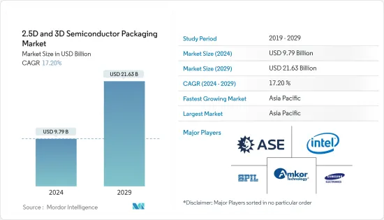
預計2024年全球2.5D/3D半導體封裝市場規模為97.9億美元,2029年達到216.3億美元,在預測期內(2024-2029年)複合年成長率預計為17%。
2.5D/3D是一種在一個封裝內安裝多個IC的封裝方法。 2.5D 結構將多個主動半導體晶片並排放置在矽中介層上,以實現高晶粒間互連密度。 3D 架構透過晶粒堆疊來整合主動晶片,以實現最短的互連和最小的封裝佔用空間。近年來,2.5D/3D憑藉其極高的封裝密度和能源效率的優勢,作為理想的晶片組整合平台獲得了發展勢頭。
主要亮點
- 高效能運算、資料中心網路和自動駕駛汽車正在推動該市場的採用率並加速技術發展。趨勢是在雲端、邊緣運算和設備層面擁有更大的運算資源。此外,通訊和基礎設施行業中高階性能應用和人工智慧 (AI) 的成長也推動了市場的發展。
- 數位化的不斷發展、遠端工作和遠端控制的趨勢不斷增強,以及消費者對電子產品的需求不斷增加,都推動了對能夠實現各種新功能的先進半導體設備的需求。隨著對半導體元件的需求不斷成長,先進的封裝技術提供了當今數位化位世界所需的外形規格和處理能力。
- 資訊科技正在徹底改變現代消費者和產品消費模式。曾經僅由電氣和機械組件組成的產品,尤其是電子產品,現在是以多種方式結合硬體、軟體、感測器、微處理器、資料儲存、微處理器和連接的複雜系統,因此變得越來越流行。
- 根據每個行業的要求,2.5D 和 3D 半導體封裝單元的設計、開發和安裝需要相當高的初始投資。 3D 半導體封裝的主要成本因素包括通孔 (TSV) 形成產量比率損失、晶圓凸塊、TSV 暴露、組裝產量比率、FOEL 和 BOEL。
- 據美國預算辦公室稱,美國國防支出預計每年都會增加,直到 2033 年。 2023年美國國防支出達7,460億美元。該預測還預測,到 2033 年,這一數字將增加至 1.1 兆美元。增加全球國防預算可能為所研究市場的成長提供有利可圖的機會。
2.5D/3D半導體封裝市場趨勢
通訊和電訊終端用戶產業預計將佔據主要市場佔有率
- 通訊和電訊是市場成長最快的領域之一。世界各地產生的資料量正在迅速增加。許多嵌入式設備推動了資料的爆炸性成長,這些設備為每筆交易產生少量資料,最終形成巨量資料。組織從各種來源收集資料,包括智慧 (IoT) 設備、商業交易、工業設備和社交媒體。
- 世界各地的組織都尋求透過快速處理資料和採取行動來獲利。高效能運算 (HPC) 使公司能夠擴展運算規模,以建立可以利用大量資料的深度學習演算法。隨著更多資料的出現,對大量運算資源的需求也隨之出現,導致 HPC 得到更大程度的採用並推動市場成長。高效能運算的激增推動了對半導體設備的需求,這些設備可提供更高的性能、更低的延遲、更高的頻寬和能效,從而對 2.5D 和 3D 封裝技術產生巨大需求。
- 通訊基地台在確保行動電話和智慧型手機等行動裝置的強大通訊生態系統方面發揮著至關重要的作用。由於高頻率,5G 技術有潛力以令人難以置信的速度有效管理大量資料,因此需要更密集的基地台網路。與4G LTE相比,5G基地台具有更多的發射天線和組件,導致功耗和發熱增加。
- 根據GSMA預測,到2025年,5G行動連線預計將分別佔韓國和日本總連線的73%和68%。到 2030 年,海灣合作理事會國家約 95% 的行動連線將是 5G,亞洲 93% 的行動連線將是 5G。 5G 智慧型手機和網路的日益普及將創造新的市場機會。
- 在 5G 及其後續技術的推動下,通訊業不斷提高資料通訊速度。這些技術創新需要強大的基礎設施來管理資料量的指數成長。公司可以使用2.5D和3D封裝來開發高效能處理器和網路設備,以滿足業界不斷升級的要求。
中國預計將經歷顯著成長
- 透過使用設計緊湊的通訊晶片,技術進步促進了各種家用電器、醫療設備、通訊設備和汽車的複雜化和小型化,這推動了中國市場的需求。
- 隨著5G服務的推出,該國對智慧型手機的需求不斷增加,預計將在預測期內推動市場成長。連網型設備、支援 5G 的智慧型手機的成長以及該國消費性電子產品生產的巨大製造能力正在推動市場成長。
- 據工信部稱,中國5G基礎設施正在快速成長,到年終將擁有338萬個基地台。透過大力投入和積極部署策略,中國已實現5G廣泛覆蓋。預測到 2024 年,將安裝超過 600 萬個基地台。該地區 5G 的不斷普及預計將推動對 5G 設備的需求,從而增加中國對 2.5D 和 3D 半導體封裝的需求。
- 政府投資和私營部門產品開發的成長,以提高半導體元件的效率並支持對節能電子設備不斷成長的需求,預計將支持市場成長。
- 例如,2023年8月,國內基礎研究和前沿開拓的主要資助來源-國家自然科學基金委員會(NSFC)計劃一項新的計畫已經啟動。這將支援半導體封裝的進步,並為在中國2.5D和3D半導體封裝市場營運的供應商創造機會。
- 中國市場龐大的製造能力、現有的工業基礎設施以及半導體裝置製造的優先地位可能會支持市場成長。
- 例如,2024年5月,中國設立了第三個也是最大的國有半導體投資基金,總規模達475億美元,以加倍努力建立國內晶片產業。預計這將支持該國對 2.5D 和 3D 半導體封裝的需求,以滿足為半導體設備提供保護外殼的應用。
- 因此,政府加強國家半導體生態系統的舉措的增加以及該國作為汽車和消費電子行業全球生產商的崛起可能會支持市場成長。
2.5D/3D半導體封裝產業概況
由於跨國公司和中小型公司的存在,2.5D/3D半導體市場正在變得半固體。該市場的主要企業包括日月光集團、Amkor Technology Inc.、英特爾公司、三星電子和 Siliconware Precision Industries (SPIL)。市場上的公司正在採取收購和聯盟等策略來加強其產品陣容並獲得永續的競爭優勢。
- 2024年4月,三星的AVP團隊訂單了NVIDIA AI晶片先進封裝的契約,使該公司能夠供應未來的高頻寬記憶體晶片。三星電子的AVP團隊可能負責提供內插器和2.5D封裝技術來封裝NVIDIA的AI處理器。然而,這些處理器中使用的HBM和GPU晶片可能來自其他供應商。 2.5D封裝技術使得CPU、GPU、HBM等晶片能夠水平整合內插器上。
- 2023 年 10 月,日月光科技控股公司日月光 (Advanced Semiconductor Engineering Inc.) 宣布推出整合設計生態系統 (IDE)。此協同設計工具集旨在系統地增強 VIPack 平台上的高級封裝架構。這種新方法可以實現從單晶粒SoC 到多晶片分解 IP 區塊(例如小晶片和記憶體)的平穩過渡,以便使用 2.5 維或高階扇出結構進行整合。
其他好處:
- Excel 格式的市場預測 (ME) 表
- 3 個月分析師支持
目錄
第1章簡介
- 研究假設和市場定義
- 調查範圍
第2章調查方法
第3章執行摘要
第4章市場洞察
- 市場概況
- 產業吸引力-波特五力分析
- 供應商的議價能力
- 買方議價能力
- 新進入者的威脅
- 替代品的威脅
- 競爭公司之間的敵對關係
- 價值鏈分析
- 市場宏觀走勢分析
第5章市場動態
- 市場促進因素
- 多個產業擴大半導體裝置消費
- 對小型和高性能電子設備的需求不斷成長
- 市場限制因素
- 半導體IC設計初始投資高、複雜
- 市場機會
- 高階運算、伺服器和資料中心的採用增加
第6章 市場細分
- 依封裝技術
- 3D
- 2.5D
- 3D 晶圓級晶片級封裝 (WLCSP) - 定性分析
- 按最終用戶產業
- 家電
- 醫療設備
- 通訊/電訊
- 車
- 其他最終用戶產業
- 按地區
- 美國
- 中國
- 台灣
- 韓國
- 日本
- 歐洲
- 拉丁美洲
- 中東/非洲
第7章 競爭格局
- 公司簡介
- ASE Group
- Amkor Technology Inc.
- Intel Corporation
- Samsung Electronics Co. Ltd
- Siliconware Precision Industries Co. Ltd(SPIL)
- Powertech Technology Inc.
- Jiangsu Changjiang Electronics Technology Co. Ltd
- TSMC Limited
- GlobalFoundries Inc.
- Tezzaron Semiconductor Corporation.
第8章投資分析
第9章 市場未來展望
The 2.5D & 3D Semiconductor Packaging Market size is estimated at USD 9.79 billion in 2024, and is expected to reach USD 21.63 billion by 2029, growing at a CAGR of 17.20% during the forecast period (2024-2029).
2.5D and 3D are packaging methodologies that include multiple ICs inside the package. In a 2.5D structure, multiple active semiconductor chips are placed side-by-side on silicon interposers to achieve high die-to-die interconnect density. In a 3D structure, active chips are integrated by die stacking for the shortest interconnect and smallest package footprint. In recent years, 2.5D and 3D have gained momentum as ideal chipset integration platforms due to their merits in achieving extremely high packaging density and energy efficiency.
Key Highlights
- High-performance computing, data center networking, and autonomous vehicles are pushing the adoption rates for the market studied and accelerating its technological evolution. The trend is to have more enormous computing resources at the cloud, edge computing, and device levels. The advancements in the market studied are also possible due to the growth in high-end performance applications and artificial intelligence (AI) in the telecom and infrastructure industry.
- Rising digitization, increasing trends of remote work and remote operations, and increasing consumer demand for electronics have sparked the need for advanced semiconductor devices that enable various new capabilities. As the demands for semiconductor devices intensify consistently, advanced packaging techniques provide the form factor and processing power required for today's digitized world.
- Information technology is revolutionizing the consumption pattern of modern consumers and products. Once composed solely of electrical and mechanical parts, products, especially electronic ones, are increasingly becoming complex systems that combine hardware, software, sensors, microprocessors, data storage, microprocessors, and connectivity in myriad ways, providing more functionalities to the resulting electronic devices.
- Significantly high initial investment is required in the design, development, and setting up of 2.5D/3D semiconductor packaging units as per the requirements of different industries. The major cost-driving processes of 3D semiconductor packaging include Through Silicon Via (TSV) creation yield loss, Wafer bumping, TSV reveals, Assembly yield, FOEL, BOEL, etc.
- According to the US Congressional Budget Office, defense spending in the United States was predicted to increase yearly until 2033. Defense outlays in the United States amounted to USD 746 billion in 2023. The forecast predicted an increase to USD 1.1 trillion in 2033. The increasing defense budgets globally are likely to offer lucrative opportunities for the growth of the market studied.
2.5D and 3D Semiconductor Packaging Market Trends
Communications and Telecom End-user Industry is Expected to Hold Significant Market Share
- Communications and telecom represent one of the fastest-growing segments of the market. The amount of data generated worldwide is increasing at a rapid pace. The explosion of data is fueled by many embedded devices that produce a small amount of data for each discrete transaction and add up to big data when clubbed together. Organizations collect data from various sources, including smart (IoT) devices, business transactions, industrial equipment, social media, etc.
- Organizations worldwide are looking to benefit from processing and acting upon data quickly. High-performance computing (HPC) has enabled businesses to scale computationally to build deep-learning algorithms that may take advantage of high volumes of data. As more data emerges, the need for more significant amounts of computing resources emerges, leading to greater adoption of HPC, which drives the market's growth. With the proliferation of high-performance computing, there is an escalating demand for semiconductor devices that deliver enhanced performance, lower latency, increased bandwidth, and power efficiency, creating significant demand for 2.5D and 3D packaging technologies.
- Communication base stations play a pivotal role in ensuring a robust communication ecosystem for mobile devices, including phones and smartphones. Given its high frequencies, 5G technology may efficiently manage vast data volumes at remarkable speeds, requiring a denser network of base stations. In contrast to 4G LTE, 5G base stations feature more transmitting antennas and components, leading to increased power consumption and heat generation.
- According to the GSMA, in 2025, the share of 5G mobile connections of total connections in South Korea and Japan are anticipated to account for 73% and 68%, respectively. About 95% of mobile connections will be 5G by 2030 in GCC states and 93% in Asia. The increasing adoption of 5G smartphones and networks creates new market opportunities.
- The telecom industry continually advances data transmission speeds, driven by technologies such as 5G and its successors. These innovations demand robust infrastructure to manage the surge in data volumes. Companies may use 2.5D and 3D packaging to develop high-performance processors and network equipment, meeting the industry's escalating requirements.
China Expected to Witness Significant Growth
- Advancing technologies have contributed to the advancement and miniaturization of various consumer electronics, medical devices, telecom and communication devices, and automobiles by using compactly designed semiconductor chips, which would fuel the demand for the market in China.
- With the launch of 5G services in the country, smartphone demand has been increasing in China, which is likely to fuel the market's growth during the forecast period. The growth of connected devices, 5G-enabled smartphones, and the country's large manufacturing capabilities in the production of consumer electronic products are fueling the market's growth.
- According to MIIT, China's 5G infrastructure surged, boasting 3.38 million base stations by the close of 2023. Bolstered by substantial investments and aggressive deployment strategies, the nation achieved broad 5G coverage. Projections indicated a climb to over six million base stations by 2024. The rising execution of 5G in the region is also anticipated to boost the need for 5G-enabled devices, thereby increasing the demand for 2.5D and 3D semiconductor packaging in China.
- The growth of governmental investments and private players' product development to increase the efficiency of semiconductor components and support the increasing demand for energy-efficient electronic devices would support the market's growth.
- For instance, in August 2023, the National Natural Science Foundation of China (NSFC), a primary domestic funding source for basic research and frontier exploration, launched a new program to finance dozens of projects focused on chiplet technology. This would support the advancement in semiconductor packing and create an opportunity for market vendors operating in the country's 2.5D and 3D semiconductor packaging market.
- The Chinese market's large manufacturing capabilities, the existing industrial infrastructure, and the priority of the country's manufacturing of semiconductor devices would support the market's growth.
- For instance, in May 2024, China set up its third and largest state-backed semiconductor investment fund, worth USD 47.5 billion, as the country redoubled its efforts to build its domestic chip industry, which would support the demand for the 2.5D and 3D semiconductor packaging in the country due to its application in providing a protective enclosure for semiconductor devices.
- Therefore, the growth of governmental initiatives to strengthen the country's semiconductor ecosystem and the country's emergence as a global producer of the automotive and consumer electronic sectors would support the market's growth.
2.5D and 3D Semiconductor Packaging Industry Overview
The 2.5D & 3D Semiconductor market is semi-consolidated due to the presence of global players and small and medium-sized enterprises. Some major players in the market are ASE Group, Amkor Technology Inc., Intel Corporation, Samsung Electronics Co. Ltd, and Siliconware Precision Industries Co. Ltd (SPIL). Players in the market are adopting strategies such as acquisitions and partnerships to enhance their product offerings and gain sustainable competitive advantage.
- In April 2024, Samsung's AVP team received an order for advanced packaging for NVIDIA's AI chip, allowing for the future supply of high-bandwidth memory chips. The AVP team at Samsung Electronics may be responsible for providing interposer and 2.5D packaging technology for packaging NVIDIA's AI processors. However, the HBM and GPU chips used in these processors may come from other suppliers. 2.5D packaging technology allows for the horizontal integration of chips such as CPUs, GPUs, and HBMs on an interposer.
- In October 2023, Advanced Semiconductor Engineering Inc., a part of ASE Technology Holding Co. Ltd, introduced its Integrated Design Ecosystem (IDE). This collaborative design toolset aims to enhance advanced package architecture on its VIPack platform systematically. This new approach enables a smooth shift from a single-die SoC to multi-die disaggregated IP blocks like chiplets and memory for integration utilizing 2.5D or advanced fanout structures.
Additional Benefits:
- The market estimate (ME) sheet in Excel format
- 3 months of analyst support
TABLE OF CONTENTS
1 INTRODUCTION
- 1.1 Study Assumptions and Market Definition
- 1.2 Scope of the Study
2 RESEARCH METHODOLOGY
3 EXECUTIVE SUMMARY
4 MARKET INSIGHTS
- 4.1 Market Overview
- 4.2 Industry Attractiveness - Porter's Five Forces Analysis
- 4.2.1 Bargaining Power of Suppliers
- 4.2.2 Bargaining Power of Buyers
- 4.2.3 Threat of New Entrants
- 4.2.4 Threat of Substitutes
- 4.2.5 Intensity of Competitive Rivalry
- 4.3 Value Chain Analysis
- 4.4 Analysis of Macroeconomic Trends on the Market
5 MARKET DYNAMICS
- 5.1 Market Drivers
- 5.1.1 Growing Consumption of Semiconductor Devices Across Several Industries
- 5.1.2 Increasing Demand for Compact, High Functionality Electronic Devices
- 5.2 Market Restraints
- 5.2.1 High Initial Investment and Increasing Complexity of Semiconductor IC Designs
- 5.3 Market Opportunities
- 5.3.1 Growing Adoption of High-end Computing, Servers, and Data Centers
6 MARKET SEGMENTATION
- 6.1 By Packaging Technology
- 6.1.1 3D
- 6.1.2 2.5D
- 6.1.3 3D Wafer-level chip-scale packaging (WLCSP) - Qualitative Analysis
- 6.2 By End-user Industry
- 6.2.1 Consumer Electronics
- 6.2.2 Medical Devices
- 6.2.3 Communications and Telecom
- 6.2.4 Automotive
- 6.2.5 Other End-user Industries
- 6.3 By Geography
- 6.3.1 United States
- 6.3.2 China
- 6.3.3 Taiwan
- 6.3.4 South Korea
- 6.3.5 Japan
- 6.3.6 Europe
- 6.3.7 Latin America
- 6.3.8 Middle East & Africa
7 COMPETITIVE LANDSCAPE
- 7.1 Company Profiles
- 7.1.1 ASE Group
- 7.1.2 Amkor Technology Inc.
- 7.1.3 Intel Corporation
- 7.1.4 Samsung Electronics Co. Ltd
- 7.1.5 Siliconware Precision Industries Co. Ltd (SPIL)
- 7.1.6 Powertech Technology Inc.
- 7.1.7 Jiangsu Changjiang Electronics Technology Co. Ltd
- 7.1.8 TSMC Limited
- 7.1.9 GlobalFoundries Inc.
- 7.1.10 Tezzaron Semiconductor Corporation.
8 INVESTMENT ANALYSIS
9 FUTURE OUTLOOK OF THE MARKET
 2025 年至 2033 年半導體封裝市場規模、佔有率、趨勢及預測(按類型、封裝材料、技術、最終用戶和地區)
 2025年先進晶片封裝全球市場報告
 半導體封裝:市場佔有率分析、產業趨勢與統計、成長預測(2025-2030 年)面板級封裝:市場佔有率分析、產業趨勢與統計資料、成長預測(2025-2030 年)
 3-D TSV:關鍵問題洞察與市場分析
 高密度封裝(MCM、MCP、SIP、3D-TSV):市場分析與技術趨勢2025 年 3D 半導體封裝全球市場報告
 先進半導體封裝市場:未來預測(2025-2030)
 半導體封裝市場規模、佔有率和成長分析(按材料、封裝技術、最終用途行業和地區)- 2025-2032 年行業預測全球 MEMS 封裝 -市場佔有率分析、產業趨勢/統計、成長預測(2025-2030 年)