


 |
市場調查報告書
商品編碼
1687872
面板級封裝:市場佔有率分析、產業趨勢與統計資料、成長預測(2025-2030 年)Panel Level Packaging - Market Share Analysis, Industry Trends & Statistics, Growth Forecasts (2025 - 2030) |
||||||
※ 本網頁內容可能與最新版本有所差異。詳細情況請與我們聯繫。
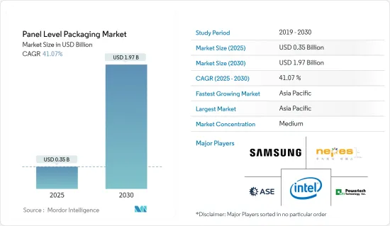
面板級封裝市場規模預計在 2025 年為 3.5 億美元,預計到 2030 年將達到 19.7 億美元,預測期內(2025-2030 年)的複合年成長率為 41.07%。
半導體產業正在經歷快速成長,半導體成為所有現代技術的基本組成部分。該領域的進步和創新直接影響所有下游技術,推動市場研究的需求。
關鍵亮點
- 隨著半導體產業重要性的不斷成長,對增強型封裝解決方案的需求也日益成長,從而推動了新型半導體封裝技術的發展。
- 面板級封裝(PLP)是一項最近備受關注的技術。 PLP是指以面板尺寸加工的半導體封裝。在面板級封裝中,組裝過程包括面板級的晶片貼裝、重新佈線、成型和凸塊製造。
- 由於採用面板平行格式處理大量封裝,因此與圓形晶圓形式相比,這種封裝類型有利於實現更好的面積利用率(面板/晶圓尺寸與封裝尺寸的比率)。因此,降低包裝成本是市場成長的主要驅動力之一。 PLP 對環境的影響也很小,因為它產生的廢棄物較少,留下的碳足跡也較少。
- 面板級封裝(PLP)市場並不缺乏挑戰。該技術的巨大成本及其實施的複雜性可能會阻礙其廣泛接受。封裝製程有兩種:先塑封 (mold 領先)和先RDL (RDL 領先)。然而,某些類型的封裝可能會導致晶片移位問題。晶片移位被認為是最大的問題之一,因為它會降低產量比率並對產量比率負面影響。這導致對包裝過程的控制需求不斷增加,增加了複雜性並抑制了市場成長。
- 在新冠疫情 (COVID-19) 之後,我們預計由於成本效益以及封裝尺寸從晶圓到大面板格式的擴展,面板級封裝將受到更多關注。並行生產的封裝數量不斷增加也是支持市場成長的一大優勢。 PLP 可能會採用其其他技術部門的製程、材料和設備。印刷電路基板(PCB)、液晶顯示器(LCD)、太陽能設備等都是以面板尺寸製造的,為扇出面板級封裝提供了一種新方法。
面板級封裝市場趨勢
市場區隔以消費性電子領域為主
- 智慧型手機、穿戴式裝置、平板裝置等家用電子電器產品正變得越來越薄、越來越小。 PLP 滿足了對更小、更輕的組件的需求,使製造商能夠提高組件密度並更有效地利用空間。對於這些設備,PLP 提供的減少的佔用空間對於實現時尚的設計和最大限度地利用可用空間至關重要。
- 家用電子電器產業與力求產品差異化的製造商競爭。 PLP 可實現家用電子電器更時尚的設計、更強大的功能和更佳的效能,從而為您帶來市場優勢。為了維持市場地位,製造商正在使用 PLP 來滿足消費者需求並推出創新產品。
- 近年來,5G和物聯網的日益普及為市場帶來了巨大的成長機會。例如,根據5G Americas的預測,全球5G用戶數將在2024年達到28億,2027年達到59億。
- 隨著對 5G 的投資不斷成長,對支援 5G 的智慧型手機的需求也在同步成長。根據 CyberMedia Research 的報告,自 2020 年首次推出以來,5G 智慧型手機銷量成長了 13 倍,到 2023 年底,5G 智慧型手機出貨量預計將以每年 70% 的速度成長。 5G 智慧型手機市場佔有率在 2020 年僅為 4%,預計到 2023 年將達到 45%。
- 同樣,由於物聯網 (IoT) 的日益普及,近年來連接設備的數量也迅速成長,物聯網是一種使事物和人們能夠使用網際網路和 IP通訊協定進行通訊的技術。例如,根據思科預測,到2023年,連網設備數量將達到293億台。物聯網用例的大幅擴展預計將成為市場成長的主要驅動力。
中國可望引領市場
- 中國是最大的半導體消費國,這主要得益於其國內電子產品市場的規模。中國是世界上最大的家用電子電器生產國和出口國,許多全球供應商已在該國設立工廠,以利用其低廉的勞動力成本。
- 電子製造業近年來也穩定擴張。根據工業信部報告,2023年電子資訊製造業主要企業工業增加價值年平均成長3.4%。根據工信部統計,主要產品中,行動電話產量15.7億部,與前一年同期比較去年成長6.9%。其中,智慧型手機產量11.4億部,與前一年同期比較增1.9%。近年來,政府採取了多項措施來促進電子產業的發展。
- 中國在5G部署方面也處於世界領先地位。據工業和資訊化部稱,中國的目標是到 2023 年 2 月擁有 5.9201 億 5G 用戶。預計到 2025 年,這一數字將超過 10 億。中國正在進行基礎設施建設,以擴大 5G 在全國的覆蓋範圍。
- 例如,截至2023年10月,中國擁有約322萬個5G基地台,佔行動基地台總數的28.1%。
- 隨著5G在國內的推廣與推進,5G設備的普及率也不斷提高。例如,根據中國資訊通訊研究院(CAICT)的預測,2023年中國5G智慧型手機出貨量將達到2.4億部,與前一年同期比較成長約11.9%,而整體智慧型手機出貨量市場將比與前一年同期比較成長約1.1%。由於先進的封裝技術可以幫助滿足 5G 晶片的許多性能要求,預計這一趨勢將有利於該國研究市場的成長。
- 此外,中國在汽車生產和消費方面均處於領先地位,預計這將有利於該國的市場成長。對更清潔、更安全的汽車的需求不斷成長是該國汽車行業的主要趨勢之一,推動了市場的成長。自動駕駛汽車、電氣化、座艙豐富化、連接性和軟體定義以及區域架構等市場大趨勢也在支持汽車領域的市場成長。
面板級封裝產業概覽
面板級封裝市場處於半固體狀態,主要參與者包括三星電子、英特爾公司、Nepes 公司、ASE 集團和 Powertech Technology Inc.。市場參與企業正在採取聯盟和收購等策略來加強其產品供應並獲得永續的競爭優勢。
- 2023年12月-NEPES開發用於邊緣運算的智慧半導體「METIS」。 Metis 採用了 Nepes 最先進的 2.5D 和 3D 封裝平台 nePAC™ 的 cx-BGA(球柵陣列)。 nePACTM是基於扇出型和覆晶鍵合技術實現多層、精細RDL佈線的下一代尖端封裝技術。適用於人工智慧半導體等高整合、高性能晶片。
- 2023年6月,日月光科技控股子公司USI在波蘭設立工廠。此舉反映出歐洲客戶對該公司產品的需求不斷成長。此次擴張將使 USI 能夠在波蘭生產更多產品,以滿足客戶需求並跟上市場成長。
其他福利
- Excel 格式的市場預測 (ME) 表
- 3個月的分析師支持
目錄
第1章 引言
- 研究假設和市場定義
- 研究範圍
第2章調查方法
第3章執行摘要
第4章 市場洞察
- 市場概覽
- 產業吸引力-波特五力分析
- 供應商的議價能力
- 買家的議價能力
- 新進入者的威脅
- 替代品的威脅
- 競爭對手之間的競爭強度
- 產業價值鏈/供應鏈分析
- 評估宏觀經濟因素對市場的影響
第5章市場動態
- 市場促進因素
- 降低包裝過程的成本
- 對緊湊、高功能電子設備的需求不斷成長
- 增加研發投入
- 市場限制
- 包裝工藝日益複雜
第6章市場區隔
- 產業應用
- 消費性電子產品
- 車
- 通訊
- 其他工業應用
- 按地區
- 美國
- 中國
- 韓國
- 台灣
- 日本
- 歐洲
- 其他
第7章競爭格局
- 公司簡介
- Samsung Electronics Co. Ltd
- Intel Corporation
- Nepes Corporation
- ASE Group
- Powertech Technology Inc.
- Fraunhofer Institute for Reliability and Micro integration IZM
- Unimicron Technology Corporation
- DECA Technologies Inc.
- JCET/STATSChipPAC
第8章投資分析
第9章:市場的未來
The Panel Level Packaging Market size is estimated at USD 0.35 billion in 2025, and is expected to reach USD 1.97 billion by 2030, at a CAGR of 41.07% during the forecast period (2025-2030).
The semiconductor industry is witnessing rapid growth, with semiconductors emerging as the basic building blocks of all modern technology. The advancements and innovations in this field directly impact all downstream technologies and drive the need for the market studied.
Key Highlights
- With the importance of the semiconductor industry growing, the demand for enhanced packaging solutions is also increasing, leading to the development of new semiconductor packaging techniques.
- Panel-level packaging (PLP) is a technology that has gained prominence recently. PLP refers to semiconductor packaging processed on a panel size. In panel-level packaging, the assembly process includes the fabrication of die attach, redistribution lines, molding, and bumping at the panel level.
- As more packages may be processed in panel and parallel formats, this type of packaging facilitates a much better area utilization (ratio between panel/wafer size and package size) compared to round wafer shapes. Hence, a lower packaging cost is among the primary drivers for the market's growth. PLP has a lower environmental impact due to a lower waste generation and carbon footprint.
- The panel-level packaging (PLP) market also encounters certain challenges. The substantial expenses linked to the technology and the intricate nature of its implementation might impede its extensive acceptance. The packaging process involves both types, mold first and RDL first. However, the type of packaging involves problems in die shift. Shifting the die is considered one of the biggest issues as it may cause lesser yield or negatively influence the yields. This increases the need for more control over the packaging process and adds complexity, restraining the market's growth.
- In the post-COVID-19 period, the focus on panel-level packaging is anticipated to increase due to the cost benefits and the expansion of the packaging size from wafers to larger panel formats. Increasing the number of packages manufactured in parallel is another major advantage supporting the market's growth. PLP may adopt processes, materials, and equipment from other technology areas. Printed circuit boards (PCB), liquid crystal displays (LCD), or solar equipment are manufactured on panel sizes and offer new approaches for fan-out panel-level packaging.
Panel Level Packaging Market Trends
Consumer Electronics Segment to Hold Major Market Share
- Consumer electronics such as smartphones, wearables, and tablets are becoming increasingly thin and compact. To meet the needs of miniaturization and light form factors, PLP allows manufacturers to achieve greater component density and more efficient use of space. For these devices, the reduced footprint caused by PLP is essential as it will enable sleek designs and maximize their utilization of available space.
- The consumer electronics industry competes with manufacturers who strive to differentiate products. By enabling sleek designs, increased functionality, and improved performance for consumer electronics devices, PLP provides an advantage to the market. To maintain their position in the market, manufacturers take advantage of PLP to meet consumer demands and introduce innovative products.
- The increasing penetration of 5G and IoT in recent years presents significant growth opportunities for the market. For instance, as per 5G Americas, the 5G subscriptions worldwide are estimated to reach 2.8 billion in 2024 and 5.9 billion by 2027.
- With the rising investments in 5G, the demand for 5G-enabled smartphones is also increasing parallelly. According to a report from Cybermedia Research, by the end of 2023, after recording a 13 times increase in 5G smartphone sales since its first introduction in 2020, shipments of 5G smartphones increased by 70% yearly. From only 4% in 2020, 5G smartphones were projected to capture a possible 45% market share in 2023.
- Similarly, owing to the rising adoption of the Internet of Things (IoT), the technology that enables communications between things and people using the Internet and IP-enabled protocols, the number of connected devices has been increasing rapidly in recent years. For instance, as per Cisco, there would be 29.3 billion networked devices in 2023. The massive expansion in IoT use cases will provide a significant impetus to market growth.
China is Expected to Lead the Market
- China is the largest semiconductor consumer, primarily due to the size of the domestic electronics market. The country is the world's largest producer and exporter of consumer electronics, as a significantly more significant number of global vendors have established their facilities to leverage the benefits of cheap labor costs.
- The electronics manufacturing industry has also recently continued to maintain steady expansion. As per a report by the Ministry of Industry and Information Technology via China Daily, in 2023, the industrial added value of major companies in the electronic information manufacturing sector grew by 3.4% yearly. According to the ministry, among significant products, the output of mobile phones increased by 6.9% Y-o-Y to 1.57 billion units, within which the number of smartphones increased by 1.9% Y-o-Y to 1.14 billion units. Several initiatives have been taken in recent years to boost the electronics industry's growth.
- China also leads in 5G adoption globally. According to the Ministry of Industry and Information Technology (MIIT), China aims to have 592.01 million 5G users as of February 2023. This number is anticipated to surpass 1 billion mark by 2025. A combined effort is being made to develop the supporting infrastructure to expand the footprint of 5G across the country.
- For instance, as of October 2023, China had about 3.22 million 5G base stations, constituting 28.1% of its entire mobile base station.
- The growing implementation of 5G in the country has also increased the uptake of 5G-enabled devices. For instance, according to the China Academy of Information and Communications Technology (CAICT), in 2023, 5G smartphone shipments in the country grew by about 11.9% Y-o-Y to 240 million units, while the overall smartphone shipments market grew by about 1.1%, compared to the previous year. As advanced packaging technologies may help resolve many of the 5G chip performance requirements, such trends are anticipated to favor the studied market's growth in the country.
- China is also a leading automotive market in production and consumption, which is anticipated to favor the market's growth in the country. The rising demand for cleaner and safer vehicles is among the major trends in the country's automotive industry, which supports the studied market's growth. Industry megatrends, including autonomous vehicles, electrification, enriched cabins, connectivity and software definition, and zonal architecture, also support the market's growth in the automotive segment.
Panel Level Packaging Industry Overview
The panel level packaging market is semi-consolidated with the presence of major players like Samsung Electronics Co. Ltd, Intel Corporation, Nepes Corporation, ASE Group, and Powertech Technology Inc. Players in the market are adopting strategies such as partnerships and acquisitions to enhance their product offerings and gain sustainable competitive advantage.
- December 2023 - NEPES developed 'METIS,' an intelligent semiconductor for edge computing. Metis applied cx-BGA (Ball Grid Array) of nePACTM, Nepes' cutting-edge 2.5D & 3D package platform. nePACTM is a next-generation cutting-edge package technology that implements multi-layer and fine RDL wiring based on fan-out technology and flip-chip bonding technology. It is suitable for highly integrated, high-performance chips such as artificial intelligence semiconductors.
- June 2023 - USI, a subsidiary of ASE Technology Holding Co. Ltd, inaugurated another factory in Poland. This move reflects the growing need for the company's products from European customers. By expanding, USI may make more goods in Poland, meet customer needs, and keep up with market growth.
Additional Benefits:
- The market estimate (ME) sheet in Excel format
- 3 months of analyst support
TABLE OF CONTENTS
1 INTRODUCTION
- 1.1 Study Assumptions and Market Definition
- 1.2 Scope of the Study
2 RESEARCH METHODOLOGY
3 EXECUTIVE SUMMARY
4 MARKET INSIGHTS
- 4.1 Market Overview
- 4.2 Industry Attractiveness - Porter's Five Forces Analysis
- 4.2.1 Bargaining Power of Suppliers
- 4.2.2 Bargaining Power of Buyers
- 4.2.3 Threat of New Entrants
- 4.2.4 Threat of Substitute Products
- 4.2.5 Intensity of Competitive Rivalry
- 4.3 Industry Value Chain/Supply Chain Analysis
- 4.4 Assessment of Impact of Macroeconomic Factors on the Market
5 MARKET DYNAMICS
- 5.1 Market Drivers
- 5.1.1 Reduced Cost of Packaging Process
- 5.1.2 Increasing Demand for Compact and High Functionality Electronic Devices
- 5.1.3 Increased Investment on Research and Development Activities
- 5.2 Market Restraints
- 5.2.1 Complexity in Packaging Process
6 MARKET SEGMENTATION
- 6.1 By Industry Application
- 6.1.1 Consumer Electronics
- 6.1.2 Automotive
- 6.1.3 Telecommunication
- 6.1.4 Other Industry Applications
- 6.2 By Geography
- 6.2.1 United States
- 6.2.2 China
- 6.2.3 Korea
- 6.2.4 Taiwan
- 6.2.5 Japan
- 6.2.6 Europe
- 6.2.7 Rest of the World
7 COMPETITIVE LANDSCAPE
- 7.1 Company Profiles
- 7.1.1 Samsung Electronics Co. Ltd
- 7.1.2 Intel Corporation
- 7.1.3 Nepes Corporation
- 7.1.4 ASE Group
- 7.1.5 Powertech Technology Inc.
- 7.1.6 Fraunhofer Institute for Reliability and Micro integration IZM
- 7.1.7 Unimicron Technology Corporation
- 7.1.8 DECA Technologies Inc.
- 7.1.9 JCET/ STATSChipPAC
8 INVESTMENT ANALYSIS
9 FUTURE OF THE MARKET
 2025 年至 2033 年半導體封裝市場規模、佔有率、趨勢及預測(按類型、封裝材料、技術、最終用戶和地區)
 2025年先進晶片封裝全球市場報告
 半導體封裝:市場佔有率分析、產業趨勢與統計、成長預測(2025-2030 年)
 3-D TSV:關鍵問題洞察與市場分析
 高密度封裝(MCM、MCP、SIP、3D-TSV):市場分析與技術趨勢2025 年 3D 半導體封裝全球市場報告
 先進半導體封裝市場:未來預測(2025-2030)
 半導體封裝市場規模、佔有率和成長分析(按材料、封裝技術、最終用途行業和地區)- 2025-2032 年行業預測全球 MEMS 封裝 -市場佔有率分析、產業趨勢/統計、成長預測(2025-2030 年)高階半導體封裝:市場佔有率分析、產業趨勢與統計、成長預測(2025-2030 年)