


 |
市場調查報告書
商品編碼
1630179
半導體晶圓拋光研磨設備:市場佔有率分析、產業趨勢、成長預測(2025-2030)Semiconductor Wafer Polishing and Grinding Equipment - Market Share Analysis, Industry Trends & Statistics, Growth Forecasts (2025 - 2030) |
||||||
價格
※ 本網頁內容可能與最新版本有所差異。詳細情況請與我們聯繫。
簡介目錄
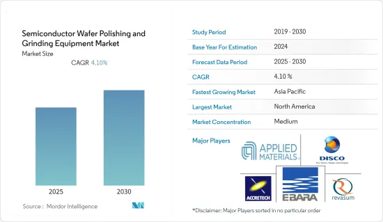
預計半導體晶圓拋光和研磨設備市場在預測期內的複合年成長率為4.1%。
主要亮點
- 對MEMS、IC製造、光學和化合物半導體的需求增加將推動半導體裝置的平坦化。在當前的市場場景下,筆記型電腦、智慧型手機、電腦等幾乎所有電子設備都採用矽IC和其他晶圓相關封裝,因此對先進研磨和拋光設備的需求不斷增加。
- 根據SEMI統計,2022年第二季全球整體矽晶圓出貨量達37.04億平方英寸,較去年同期的35.34億平方英吋成長5%。這樣的市場格局預計將在不久的將來為市場帶來一些新的機會。
- 此外,對電子設備小型化的需求不斷成長(由於對更薄且功耗更低的晶圓的需求)預計將在預測期內推動半導體晶圓拋光和研磨設備市場的若干進步。
- 然而,蝕刻技術的最新進展與拋光技術相比具有更多優勢,影響了對拋光設備的需求。此外,使用傳統 CMP(化學機械拋光)技術進行拋光來去除局部缺陷可以保留表面形貌,這使得參與晶圓回收的製造商和服務供應商變得極其困難。
- 2020 年初,COVID-19 嚴重擾亂了世界各地的半導體供應鏈和生產,尤其是在中國。然而,疫情導致的數位化趨勢日益增強,預計將增加對半導體元件的需求,並對未來市場產生正面影響。
半導體晶圓拋光研磨設備市場趨勢
消費性電子產品消費的增加預計將對市場產生正面影響
- 智慧型手機和平板電腦等家用電子電器的技術進步以及智慧家居設備和穿戴式裝置領域的發展正在推動對小型積體電路的需求。因此,在半導體晶圓製造過程中發揮重要作用的晶圓拋光和研磨設備的需求不斷增加。
- 半導體材料市場的整體需求是由智慧型手機、消費性電子和汽車等應用所推動的。這些產業受到無線技術(5G)、人工智慧等技術轉型的啟發。此外,物聯網(IoT)設備的成長趨勢預計將迫使半導體產業投資該設備以實現智慧產品。
- 所有智慧型手機均由 SoC(系統單晶片)構成,這是一種包含電腦或其他電子系統的全部或大部分組件的積體電路。 SoC 晶片通常使用金屬氧化物半導體 (MOS) 技術製造,並發送到晶圓製造工廠,在封裝和測試之前對晶圓進行拋光和研磨,以創建 SoC 晶片。因此,智慧型手機滲透率的不斷提高預計將對市場產生積極影響。
- 此外,微電子設備正在向消費性電子產品領域取得重大進展。微電子學的應用正在幫助設計穿戴在人體上的裝置。透過這種實現,腕帶、穿戴式顯示器、穿戴式醫療保健產品等旨在監測個人健康。化學機械拋光是矽晶圓製造和加工的關鍵技術,有助於實現尖端的微電子裝置和電子機械系統(MEMS)。
- 此外,高性能且輕巧的電子設備正在興起。因此,為了在此類設備中安裝更多元件,半導體必須做得更小、封裝更緊密、更輕,以便為其他元件騰出空間。因此,晶片拋光是半導體製造的重要製程。
北美預計將佔據很大佔有率
- 多年來,美國半導體產業在全球銷售市場佔有率上一直保持主導地位。該國也是半導體封裝領域的領先創新者之一,擁有遍布各州的眾多晶圓製造廠。該地區的主要無廠半導體公司包括 Broadcom、AMD、Qualcomm、Apple、Marvell、Xilinx 和 NVIDIA。
- 隨著無廠半導體公司(間接)、整合設備製造商和工廠活性化半導體晶圓製造商的活動,預計該地區在預測期內仍將是所研究市場的主要收益貢獻者之一。
- 此外,該地區消費性電子產業的擴張也是推動市場成長的關鍵因素。例如,根據 CTA 的數據,該地區的消費電子產業預計到 2022 年將產生超過 5,050 億美元的零售額,而 2021 年與 2020 年相比成長了 9.6%,令人印象深刻。
- 汽車功率半導體 IC 的成長也推動了晶圓需求。電力基礎設施投資的增加和充電站數量的增加正在推動美國半導體市場的成長。該地區也是一些投資電動車行業的世界領先汽車製造商的所在地。
- 根據美國能源部的數據,2020年至2021年電動車銷量成長了85%,插電式混合動力電動車(PHEV)銷量在2021年成長了一倍多,與前一年同期比較成長138%。半導體構成了電動車領域電氣化動力傳動系統組件(例如充電器、DC-DC 逆變器和牽引驅動逆變器)的核心要素。
半導體晶圓拋光研磨設備產業概況
半導體晶圓拋光和研磨設備市場適度整合,並由一些大型企業組成。過去20年,市場競爭力不斷增強。從市場佔有率來看,目前該市場由幾家主要企業佔據。各個供應商不斷更新現有設備以提高效率。
- 2022 年 6 月 - 應用材料公司宣布收購了總部位於芬蘭的私人半導體製造設備公司 Picosun Oy。此次收購預計將擴大應用材料公司的 ICAPS(物聯網、通訊、汽車、電力、感測器)產品系列和客戶開發。
- 2022 年 2 月 - Reversum 宣布已從 SQN Venture Partners, LLC 籌整合長資金。該貸款提供高達 800 萬美元的債務融資,以加速新產品開發並提供營運資金以支持快速成長。
其他好處:
- Excel 格式的市場預測 (ME) 表
- 3 個月的分析師支持
目錄
第1章簡介
- 研究假設和市場定義
- 調查範圍
第2章調查方法
第3章執行摘要
第4章市場動態
- 市場概況
- 產業吸引力-波特五力分析
- 新進入者的威脅
- 買方議價能力
- 供應商的議價能力
- 替代品的威脅
- 競爭公司之間敵對關係的強度
- 產業價值鏈分析
- 評估 COVID-19 對產業的影響
- 市場促進因素
- 擴大消費性電子產品消費
- 對半導體小型化的需求日益成長
- 市場挑戰
- 製造複雜性
第5章市場區隔
- 按地區
- 北美洲
- 歐洲
- 亞太地區
- 世界其他地區
第6章 競爭狀況
- 公司簡介
- Applied Materials Inc.
- Ebara Corporation
- Lapmaster Wolters GmbH
- Logitech Ltd
- Entrepix Inc.
- Revasum Inc.
- Tokyo Seimitsu Co. Ltd(Accretech Create Corp.)
- Logomatic GmbH
- Disco Corporation
- Komatsu NTC Ltd
- Okamoto Corporation
第7章 投資分析
第8章市場的未來
簡介目錄
Product Code: 59311
The Semiconductor Wafer Polishing and Grinding Equipment Market is expected to register a CAGR of 4.1% during the forecast period.
Key Highlights
- The increasing demand in MEMS, IC manufacturing, optics, and compound semiconductors will boost the planarization in semiconductor devices. In the current market scenario, as almost all electronic devices, including laptops, smartphones, computers, etc., make use of Silicon ICs and other wafer-dependent packages, the demand for advanced grinding and polishing machinery is always on the rise.
- According to SEMI, silicon wafer shipments across the world in the second quarter of 2022 saw a 5% growth reaching 3,704 million square inches from 3,534 million square inches reported during the same quarter in the previous year. Such a market scenario is expected to unlock several new opportunities for the market in the near future.
- Further, the growing need for miniaturization in electronics (due to the demand for thinner wafers that consume low power) is expected to drive some advancements in the semiconductor wafer polishing and grinding equipment market over the forecast period.
- However, the recent advancements in etching, which offer more advantages compared to polishing techniques, are affecting the demand for polishing machinery. Moreover, the removal of partial defects through polishing with traditional CMP (chemical-mechanical-polishing) technology preserves the surface profile, making it extremely difficult for manufacturers and service providers involved in wafer reclaim activities.
- Covid-19 significantly disrupted the supply chain and production of semiconductors worldwide, especially in China, during the initial phase of 2020. However, the rising trends of digitalization due to the pandemic have increased the demand for semiconductor components, which is expected to have a positive impact on the market going forward.
Semiconductor Wafer Polishing and Grinding Equipment Market Trends
Growing Consumption of Consumer Electronics is Expected to Positively Impact the Market
- The technological advancements in consumer electronic devices, such as smartphones and tablets, and the development of smart home devices and wearables globally are driving the need for small integrated circuits. This, in turn, is fueling the demand for wafer polishing and grinding equipment, which plays a crucial role in the semiconductor wafer fabrication process.
- The overall demand for the semiconductor materials market is being driven by smartphones and other applications across consumer electronics, automotive applications, etc. These industries have been inspired by technology transitions such as wireless technologies (5G), Artificial intelligence, etc. Also, the trend of increasing numbers of Internet of Things (IoT) devices is expected to force the semiconductor industry to invest in this equipment, in a bid to attain intelligent products.
- Every smartphone is comprised of a System On a Chip (SoC), which is an integrated circuit that integrates all or most components of a computer or other electronic system. SoC chips are typically fabricated using metal-oxide-semiconductor (MOS) technology and are sent to a wafer fabrication plant to create the SoC dice before packaging and testing where wafer polishing and grinding is done. As such, the growing penetration of smartphones is expected to have a positive impact on the market.
- Further, microelectronic devices have significantly permeated consumer electronics. The application of microelectronics has helped in the design of devices that are attached to the human body. Owing to this implementation, wristbands, wearable displays, and wearable healthcare products have been designed to monitor an individual's well-being. Chemical-mechanical polishing, as a key technology in the production and processing of silicon wafers, has helped in the realization of state-of-the-art microelectronic devices and micro-electro-mechanical systems (MEMS).
- Moreover, there is an emergence of electronic innovations that are becoming more powerful in performance yet lighter in weight than their predecessor. As such, for more components to fit into such devices, the semiconductors have to be smaller, tightly packed, and lighter in weight to reserve space for other elements to fit in as well. Thus, wafer grinding is a critical process for the manufacturing of semiconductors.
North America is Expected to Hold Significant Share
- Over the years, the United States semiconductor industry has maintained its leadership position in terms of the global sales market share. The country is also one of the major innovators in semiconductor packaging, boasting many wafer fabrication plants spread across different states. Some major fabless companies in this region include Broadcom, AMD, Qualcomm, Apple, Marvell, Xilinx, and NVIDIA.
- The region is likely to remain one of the major revenue contributors to the market studied over the forecast period, as fabless companies (indirect), integrated device manufacturers, and factories are increasing several activities for semiconductor wafer manufacturers.
- Moreover, the proliferating consumer electronics industry in the region is also an important factor driving the growth of the market. For instance, according to CTA, the consumer electronics industry in the region is projected to generate over USD 505 billion in retail sales revenue in 2022, representing a 2.8% revenue increase from 2021's impressive 9.6% growth over 2020.
- The demand for wafers is also due to the rise of power semiconductors ICs for automotive applications. Increasing investments in electric infrastructure and an increasing number of charging stations are boosting the growth of the semiconductor market in the US. The region is also home to some of the major automotive players in the world, which are investing in the electric car segment.
- As per the US DoE, EV sales grew by 85% from 2020 to 2021, while sales of plug-in hybrid electric vehicles (PHEVs) more than doubled in 2021, with an increase of 138% over the previous year. Semiconductors form a core element of the EV landscape for electrified powertrain components like chargers, DC to DC inverters, and traction drive inverters.
Semiconductor Wafer Polishing and Grinding Equipment Industry Overview
The semiconductor wafer polishing and grinding equipment market is moderately consolidated and consists of certain major players. The market has gained a competitive edge over the past two decades. In terms of market share, few major players dominate the market, currently. Various vendors are continually updating their existing equipment for better efficiency.
- June 2022 - Applied Materials announced that it had acquired Picosun Oy, a privately held semiconductor equipment company based in Finland. The acquisition was expected to broaden the Applied ICAPS (IoT, Communications, Automotive, Power and Sensors) product portfolio and customer engagements.
- February 2022 - Revasum announced that it had secured a growth capital facility from SQN Venture Partners, LLC. The facility would provide up to USD 8 million in debt financing to accelerate new product development and provide working capital to support rapid growth.
Additional Benefits:
- The market estimate (ME) sheet in Excel format
- 3 months of analyst support
TABLE OF CONTENTS
1 INTRODUCTION
- 1.1 Study Assumptions and Market Definition
- 1.2 Scope of the Study
2 RESEARCH METHODOLOGY
3 EXECUTIVE SUMMARY
4 MARKET DYNAMICS
- 4.1 Market Overview
- 4.2 Industry Attractiveness - Porter's Five Forces Analysis
- 4.2.1 Threat of New Entrants
- 4.2.2 Bargaining Power of Buyers
- 4.2.3 Bargaining Power of Suppliers
- 4.2.4 Threat of Substitute Products
- 4.2.5 Intensity of Competitive Rivalry
- 4.3 Industry Value Chain Analysis
- 4.4 Assessment of COVID-19 impact on the industry
- 4.5 Market Drivers
- 4.5.1 Growing Consumption of Consumer Electronics
- 4.5.2 Increasing Need for Miniaturization of Semiconductors
- 4.6 Market Challenges
- 4.6.1 Complexity Regarding Manufacturing
5 MARKET SEGMENTATION
- 5.1 Geography
- 5.1.1 North America
- 5.1.2 Europe
- 5.1.3 Asia Pacific
- 5.1.4 Rest of the World
6 COMPETITIVE LANDSCAPE
- 6.1 Company Profiles
- 6.1.1 Applied Materials Inc.
- 6.1.2 Ebara Corporation
- 6.1.3 Lapmaster Wolters GmbH
- 6.1.4 Logitech Ltd
- 6.1.5 Entrepix Inc.
- 6.1.6 Revasum Inc.
- 6.1.7 Tokyo Seimitsu Co. Ltd (Accretech Create Corp.)
- 6.1.8 Logomatic GmbH
- 6.1.9 Disco Corporation
- 6.1.10 Komatsu NTC Ltd
- 6.1.11 Okamoto Corporation
7 INVESTMENT ANALYSIS
8 FUTURE OF THE MARKET
02-2729-4219
+886-2-2729-4219
 半導體晶圓拋光和研磨設備市場按設備類型、晶圓尺寸、應用和最終用戶分類 - 2025 年至 2030 年全球預測
 2025 年至 2035 年全球半導體晶圓拋光研磨設備市場
 半導體晶圓拋光和研磨設備市場規模、佔有率、趨勢分析報告:按產品、晶圓尺寸、最終用途、地區和細分市場進行預測,2025 年至 2030 年
 半導體拋光墊市場,按類型、按應用、按材料、按國家和地區 - 2025 年至 2032 年全球行業分析、市場規模、市場佔有率和預測半導體晶圓拋光和研磨設備市場,按應用、最終用戶、國家和地區分類 - 2024-2032 年行業分析、市場規模、市場佔有率和預測半導體晶圓拋光和研磨設備市場報告(按類型(半導體晶圓拋光設備、半導體晶圓研磨設備)、最終用戶(代工廠、記憶體製造商、IDM 等)和地區 2024-2032
 2024-2028年全球半導體晶圓拋光研磨設備市場半導體拋光墊片市場報告:2030 年趨勢、預測與競爭分析
 半導體拋光墊市場 - 2023-2028年預測